I Got an Early Look at Intel's Glass Packaging Tech for Faster Chips
Advanced packaging combining lots of "chiplets" into one processor is big deal. I visited an Intel chip factory to see one way Intel hopes to engineer a new speed boost.


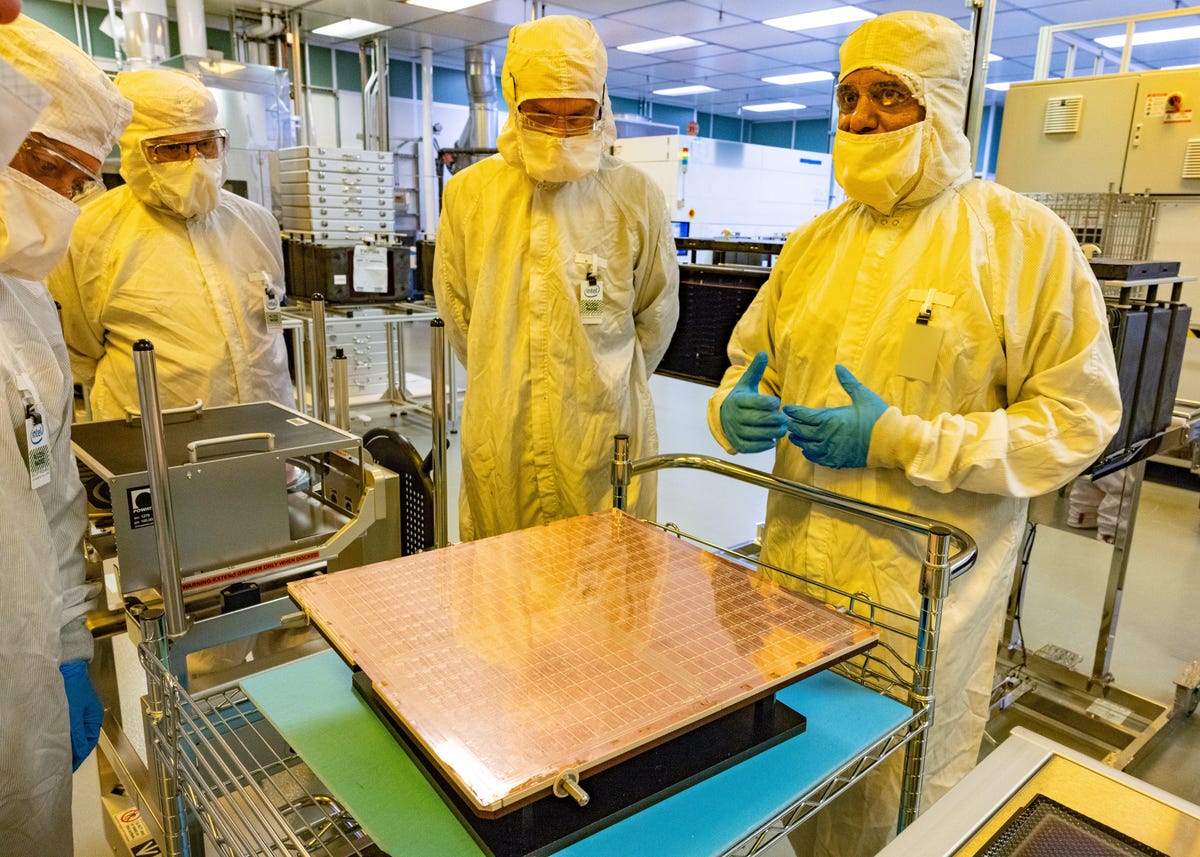
Intel glass substrate technology
Rahul Manepalli, right, Intel's module engineering leader, shows a glass substrate panel before it's sliced into the small rectangles that will be bonded to the undersides of hundreds of test processors. I was one of just two journalists who visited Intel's CH8 facility in Chandler, Arizona, to get the first look at how this technology works, and I took all the photos you'll see here.
The technology stands to improve performance and power consumption of advanced processors arriving later this decade. Glass substrates should permit physically larger processors comprising several small "chiplets" for AI and data center work, but Intel expects they'll trickle down to PCs, too.
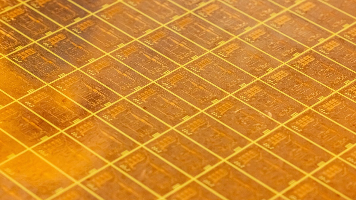
Intel glass substrate
Intel lays down patterns on glass substrates to route data and power signals through a complex 3D network between a processor and its circuit board. The company uses a variation of the lithography machines that etch circuitry onto computer chips, though not with nearly as fine a patterning resolution.

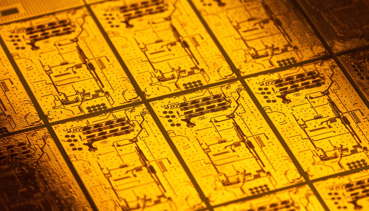
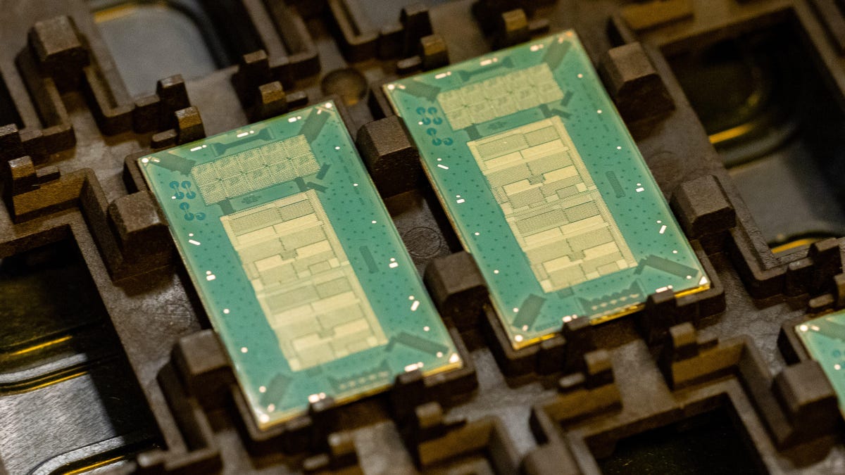
Glass substrate test chip underside
A tray holds a pair of Intel test chips mounted into a processor package using a glass substrate. One part of the substrate's job is to route data and electricity from the hundreds of yellow contacts shown here to many more on the underside of the silicon processor itself.
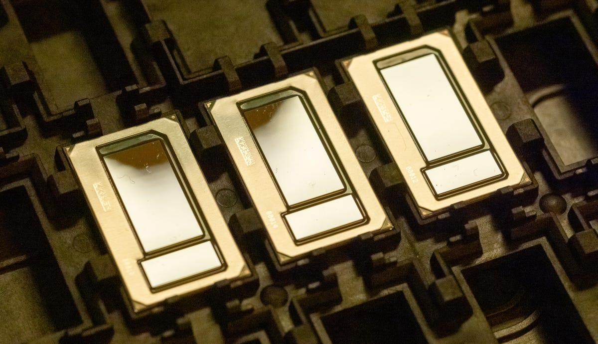
Glass substrate test processors
A tray holds a trio of test processors Intel build to evaluate its glass substrate technology, a packaging development it expects will enable much larger processors made of several interlinked chiplets.
Intel glass substrate for faster processors
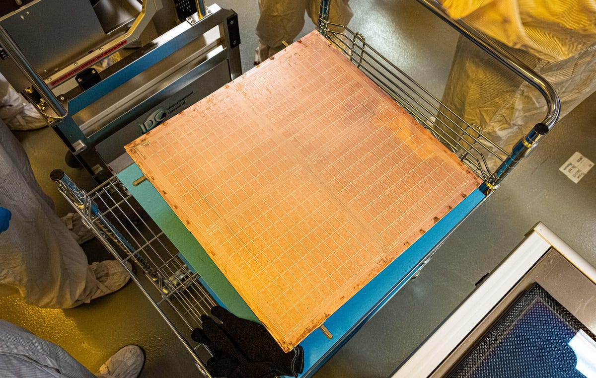
Each of these rectangles, about the size of a stubby stick of chewing gum, is a glass substrate element that fits underneath a processor to connect its power and data pathways. Intel expects the technology to be mature later this decade. This photo shows a portion of a larger glass panel measuring 510x515mm that later will be sliced up for attachment to a test chip.
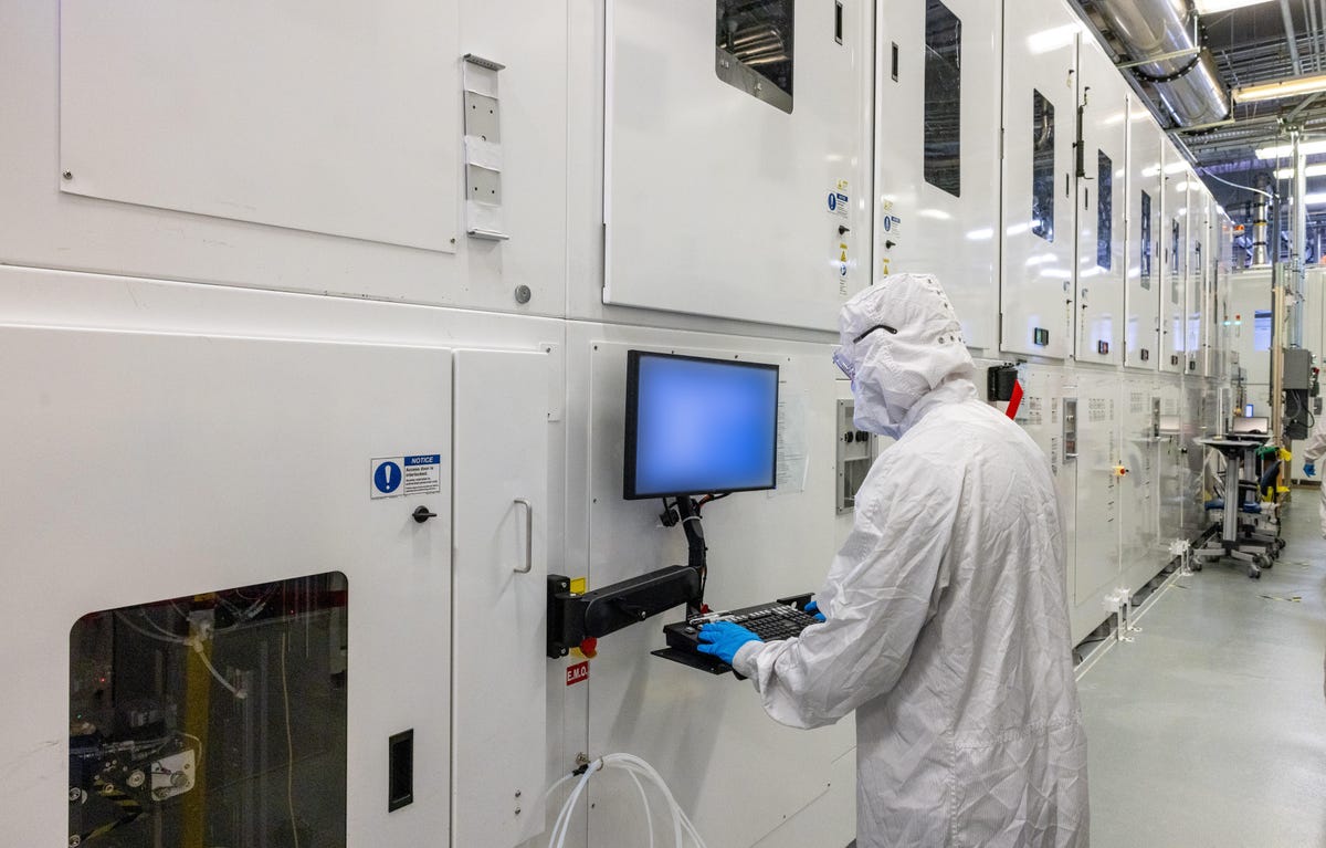
Glass substrate processing equipment
A two-story machine, sealed away from cleanroom air and longer than most buses, handles glass panels measuring 510x515mm that are transformed into complex multilayered rectangles for routing data and power to a processor.
Intel glass substrate test system
Thousands of tiny contact points look like pale yellow rectangules atop this glass substrate that later will be connected to a test chip.

Intel's Chandler, Arizona, manufacturing complex
Intel built eight major chip fabrication plants, or fabs, CH1 through CH8, in Chandler, Arizona, decades ago. It's reused many of the boxy buildings for new work, like the development of glass substrate technology in CH8. The Phoenix suburb can be scorching hot even in September.
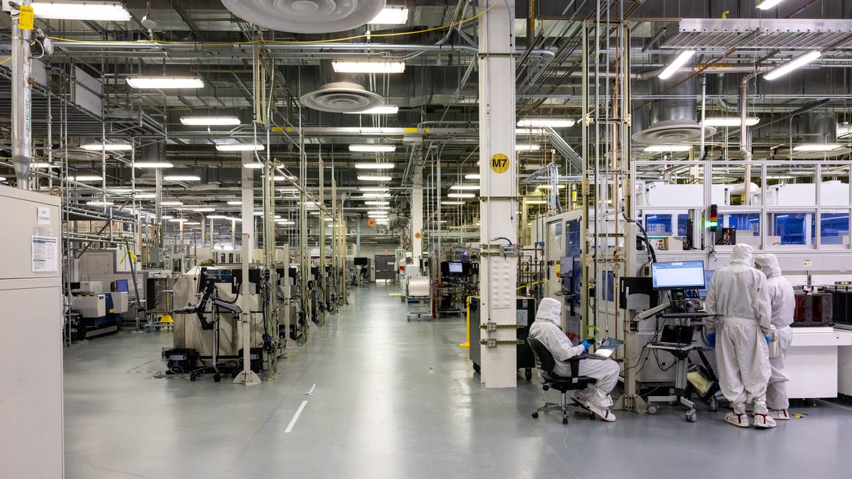
Intel CH8 substrate and packaging facility
The inside of CH8, an Intel facility in the Phoenix suburb of Chandler, Arizona, is packed with equipment for manufacturing the substrates that lie beneath processors and other packaging technology. It's where Intel developed its EMIB (embedded multidie interconnect bridge) technology in past years and is working on glass substrates today.
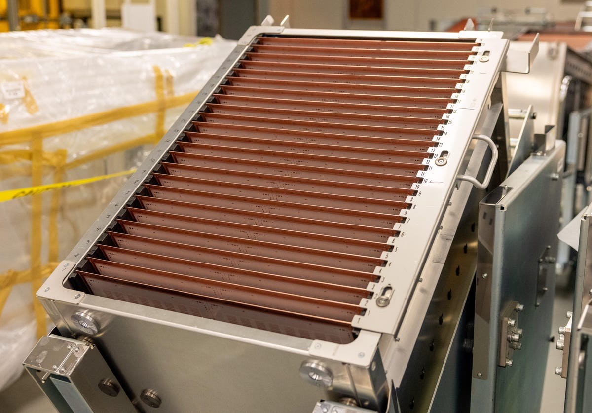
Intel organic substrates
This stack of organic substrates in Intel's CH8 facility shows a technology for packaging processors that caught on more than two decades ago. It uses an epoxy resin to connect processors to the their circuit boards. Organic substrates largely replaced ceramic substrates, and Intel and analysts expect glass will replace organic substrates in many situations.
Intel glass substrate panel
For its glass substrates, Intel reuses the 510x515mm substrate panel sizes that earlier substrates use. This substrate panel will be sliced up, one rectangle per test processor.
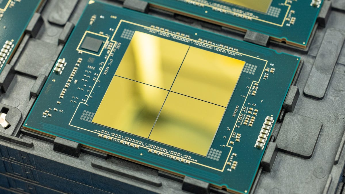
Four-die Sapphire Rapids Xeon processor
A real-world example of Intel's packaging technology is Intel's Sapphire Rapids, a large Xeon processor for data centers. Intel combines four CPU tiles, each also called a die or chiplet, into one larger processor. Intel's EMIB (embedded multidie interconnect bridge), a thin sliver of silicon underneath the edges where the tiles abut, supply data links across the processor so it behaves like one larger unit.
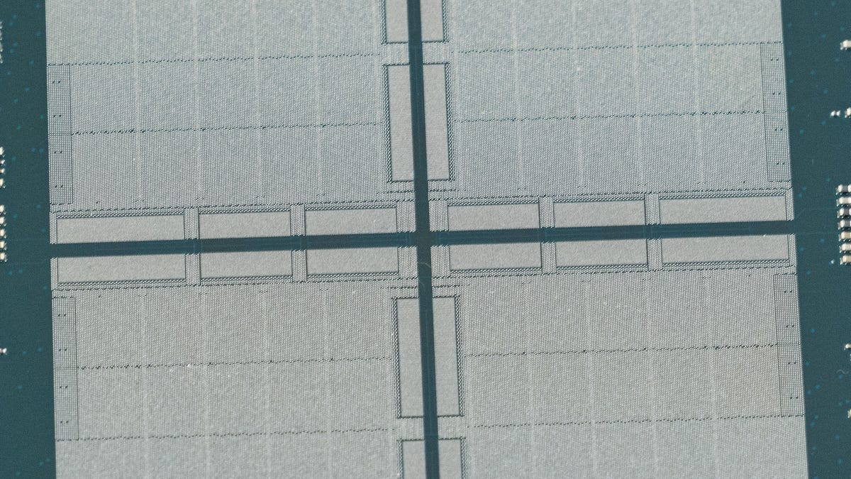
Intel Sapphire Rapids substrate
The package that houses the four Sapphire Rapids chiplets is studded with thousands of small electrical contacts for communication and power. The lighter-colored rectangles along the central crosshair shape are where EMIB communication bridges will be placed for communication links across the chiplets.
Intel advanced packaging with chiplets
This processor test package shows how Intel can link a cluster of chiplets into one larger processor. The individual chiplets can be made by different companies, with different manufacturing processes optimal for each one's cost and performance.
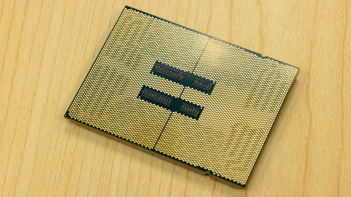
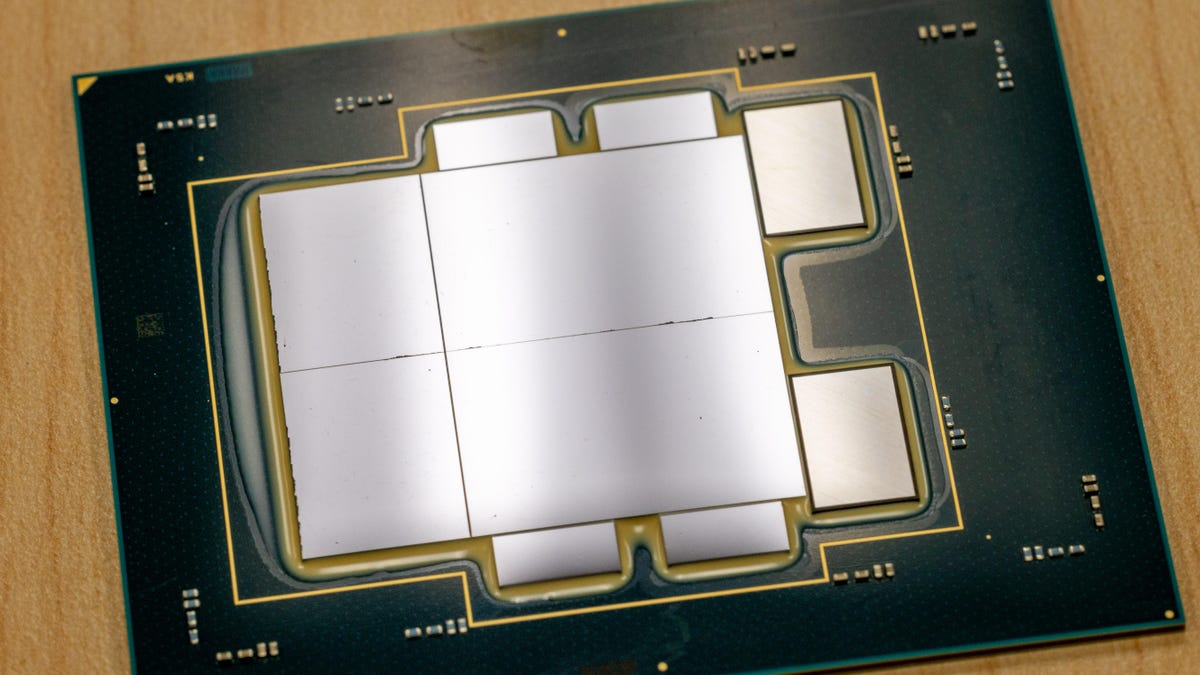
Intel Sapphire Rapids Xeon obverse
The bottom of the Sapphire Rapids Xeon chip is covered with thousands of tiny metal contact patches for data and power links. This whole package will be pressed with hundreds of pounds of force onto a circuit board to ensure good electrical contacts.
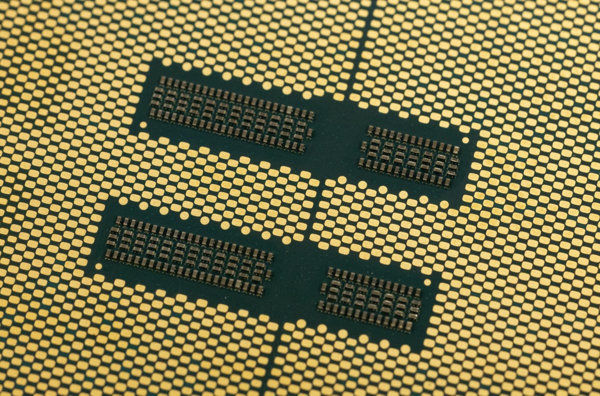
Intel Sapphire Rapids Xeon electrical contacts
This closeup photo of the bottom of the Sapphire Rapids Xeon server chip shows how densely packed the metal contact patches are for data and power links.
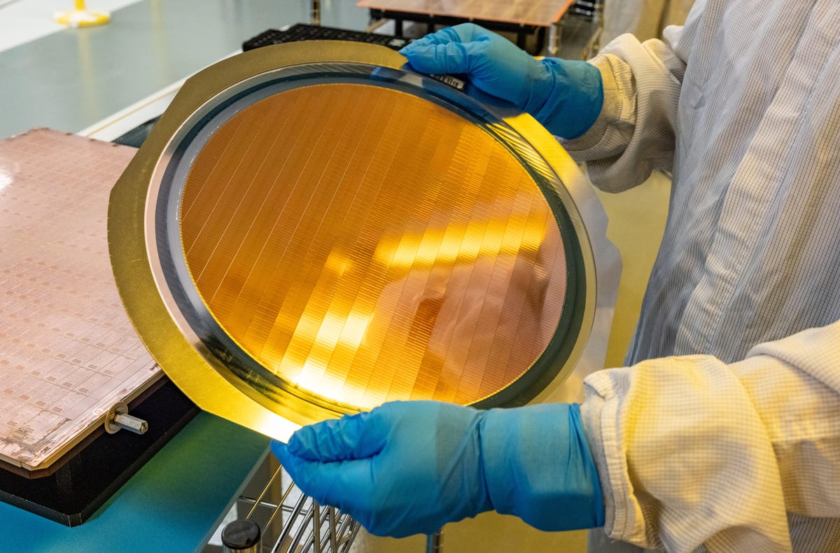
300mm silicon wafer
This is a 300mm silicon wafer, tiled with hundreds of slivers of silicon, each a tiny bridge to be tucked under adjoining processor chiplets to serve as a communications link. They're a key part of Intel's EMIB packaging technology.

EMIB communication tiles closeup
A 300mm wafer is tiled with hundreds of slivers of silicon, each a tiny silicon communication link between pairs of chiplets. Intel developed the technology, called EMIB, to help make larger processors like its Sapphire Rapids server product.
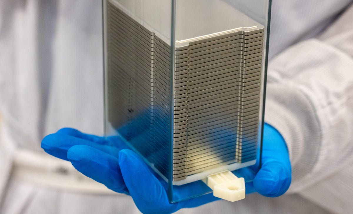
Stack of Intel heat spreaders
This plastic case houses a stack of metal heat spreaders made of nickel-plated copper. These "lids" are fitted to the top of server processors to conduct away heat to air- or water-cooling systems. Modern data center processors can draw a whopping 700 watts of power, and Intel sees kilowatt chips on the horizon, so there's a lot of heat to get rid of. The dense metal is hard to heft with just one hand.
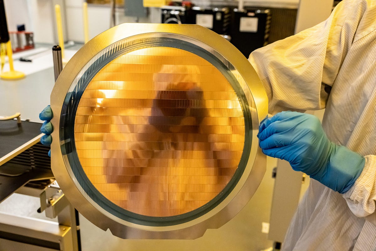
Self-portrait in Intel EMIB die
CNET reporter Stephen Shankland is reflected in a 300mm silicon wafer.
More Galleries

My Favorite Shots From the Galaxy S24 Ultra's Camera
20 Photos
Honor's Magic V2 Foldable Is Lighter Than Samsung's Galaxy S24 Ultra
10 Photos
The Samsung Galaxy S24 and S24 Plus Looks Sweet in Aluminum
23 Photos
Samsung's Galaxy S24 Ultra Now Has a Titanium Design
23 Photos
I Took 600+ Photos With the iPhone 15 Pro and Pro Max. Look at My Favorites
34 Photos