
Inside Intel's Chip Factory, I Saw the Future. It's Plain Old Glass
Intel is moving its processors to a new foundation to try to keep up with exploding demand for new computing horsepower.


- Shankland covered the tech industry for more than 25 years and was a science writer for five years before that. He has deep expertise in microprocessors, digital photography, computer hardware and software, internet standards, web technology, and more.
Computer processors are some of the most complicated devices humans ever created. Engineers pluck just the right combinations of atoms out of the periodic table to make materials that can steer cascades of electrons through billions of finely etched circuits at ultrahigh speeds.
But the next breakthrough to make our laptops more efficient and AI more powerful could come from plain old glass. I've just seen firsthand how it works.
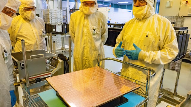
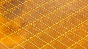
Intel will detail the glass technology at its Innovation event Tuesday in San Jose, California. I was one of just two journalists who got the first look at how this technology works, donning a stuffy head-to-toe "bunny suit" to enter Intel's ultraclean CH8 factory in Chandler, Arizona. There, in a hulking white high-tech building in the Phoenix area's scorching desert landscape, Intel transforms sheets of glass the size of a small tabletop into paperclip-sized rectangular sandwiches of circuitry built with some of the same techniques as the processor itself.
Intel has begun a years-long transition to new technology that rests processors on a bed of glass instead of today's epoxy-like organic resin. The new glass foundation, called a substrate, offers the speed, power and real estate necessary for the chip industry's shift to new technology packaging multiple "chiplets" into a single larger processor.
In short, that means a new way to sustain Moore's Law, which charts progress in cramming more circuitry elements called transistors into a processor. The A17 Pro processor in Apple's new iPhone 15 Pro has 19 billion transistors. Intel's Ponte Vecchio supercomputing processor has more than 100 billion. By the end of the decade, Intel expects processors with -- if you can imagine it -- a trillion transistors.
Intel relied on this chiplet approach to catch up to competitors with superior processor manufacturing abilities. But now Intel can use it to outpace rivals in an era when exploding demand for new processing power has surpassed the industry's ability to deliver it, said Creative Strategies analyst Ben Bajarin. And Intel's glass substrate technology demonstrates Intel's packaging prowess.
"One hundred percent, this is going to end up leading to a competitive advantage," Bajarin said.
What it means for you, a few years down the line, is supercharged laptops and AI tools that are even more stunningly smart than what you're seeing today.
Why the chip industry will shift to glass substrates
The whole chip industry will make the glass transition at least for high-end processors to cope with chipmaking challenges, and Intel has the lead, said FeibusTech analyst Mike Feibus.
With more than a decade's work collaborating with academics and testing new methods, a staff of 600 headquartered at Chandler has turned research and development into a functioning manufacturing line.
"Basically, the innovation is done," said Ann Kelleher, the executive vice president leading technology development at Intel. The glass substrate technology "gives us an ability to ultimately get higher performance for our products."
Those are bold words from a company that's halfway through a four-year effort to recover the prowess it lost to Taiwan Semiconductor Manufacturing Co. and Samsung, chip "foundries" that build processors for hundreds of electronics companies. When Intel manufacturing progress stalled for several years starting nearly a decade ago, it lost its once formidable lead to the two Asian chipmakers.
The glass technology underneath a processor won't arrive until the second half of the decade, and when it does, it'll appear first underneath the biggest, most power-hungry chips, the ones that perch in thousands of servers stacked up in data centers operated by huge "hyperscalers" like Google, Amazon, Microsoft and Meta.
That's because glass brings several advantages to these hot and huge chips, said Rahul Manepalli, an Intel fellow who leads Intel's module engineering work.
It can accommodate 10 times the power and data connections as today's organic substrates so more data can be pumped in and out of a chip. It doesn't warp as much, critical to ensuring processors lie flat and connect properly to the outside world and thus enabling 50% larger chip packages. It transmits power with less waste, meaning chips can run either faster or more efficiently. And it can run at a higher temperature, and when it heats up, it expands at the same rate as silicon to avoid mechanical failures.
Glass will enable a new generation of server and data center processors, successors to mammoth beasts like the Intel Xeons that can run cloud computing services like email and online banking and Nvidia's artificial intelligence processors that have exploded in popularity as the world embraces generative AI.
But as glass substrates mature and costs come down, it'll spread beyond data centers to the computer sitting on your lap.
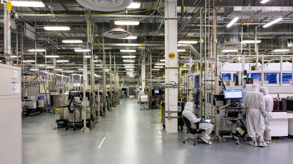
The inside of CH8, an Intel facility in the Phoenix suburb of Chandler, Arizona, is packed with equipment for manufacturing the substrates that lie beneath processors and other packaging technology. It's where Intel developed its EMIB technology in past years and is working on glass substrates today.
"Clearly we see this going into client applications," Manepalli said, using Intel's term for personal computers.
Chipmaking recovery: Five nodes in four years
Under the leadership of Chief Executive Pat Gelsinger, who rejoined Intel in 2021, Intel is trying to claw its way back to the leading edge. At every press conference and quarterly earnings call, Intel executives intone the mantra "five nodes in four years," referring to the effort to advance through five big new chip manufacturing steps at a torrid pace to catch up to TSMC and Samsung and then surpass them by 2025.
Kelleher, in charge of the effort, declares two of the steps complete so far and the rest proceeding on schedule. In a briefing I attended at Intel's Chandler facilities, with many of her top executives gathered around a conference table, the no-nonsense Irish electrical engineer makes it clear you don't want to be the person to disappoint her.
"For those who know me well, and this team may chuckle, I don't like missing a milestone," she said. The executives do indeed chuckle, but their slightly nervous tone makes it clear it's far from a joking matter.
"5N4Y," as the recovery effort is called, is a difficult, expensive and ambitious recovery plan for a company that fell so far behind. So far, Gelsinger, Kelleher and thousands of engineers are delivering the goods.
"With every passing year, I have a higher degree of confidence that they will hit those milestones," Bajarin said.
A package deal
But even if Intel recovers its lead in the manufacturing process called lithography that etches transistors onto a silicon surface, the company and its rivals all face a serious problem: building the housing that attaches those chips to a circuit board. That's where packaging and glass substrates come into the picture.
Intel's 8086 chip, the 1978 precursor to every PC and server processor that Intel has made since, was a flat square of silicon with 29,000 transistors. To protect it and plug it into a circuit board, it was housed in a package that looked like a flat caterpillar. Forty metal legs carried power and data to the chip.
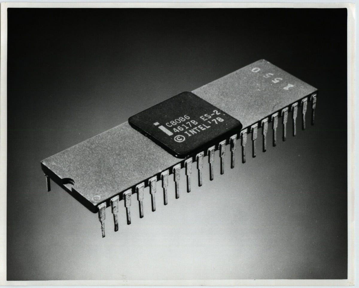
The Intel 8086 processor package had 40 electrical connections for power and data that gave the chip a caterpillar look. Modern chips have thousands of connections, now just small metal patches on the underside of the package.
Since then, processor packaging has advanced dramatically. It once was relatively crude, but now the boundary between chipmaking and packaging are blurring, Kelleher said. Packaging processes now use lithography machines to etch their own circuitry, although not nearly as finely as on processors.
Over the decades, processors moved from caterpillar legs to hundreds of pins that looked like a tiny bed of nails covering the bottom of a processor. (If you ever built a PC back in the day, slotting a processor into its socket, you'll know what I'm talking about.) But eventually that approach didn't offer enough electrical contacts to the circuit board, either.
So today's packages have flat metal contact patches on the bottom of the package. The chip is installed when hundreds of pounds of force mash it onto a circuit board.
A metal cap atop a processor draws away waste heat that otherwise would crash a computer. And beneath the processor is a substrate with an increasingly complex, three-dimensional network of power and data connections to link the chip to the outside world.
What lies beneath
There are challenges moving from today's organic substrates to glass. Glass is brittle, so it must be handled carefully, for example.
To ease the transition, Intel is adapting glass-handling equipment from experts who already know how to handle it without breaking: the display industry, which makes everything from tiny smartwatch screens to enormous flat-panel TVs. They also have to etch circuitry onto glass and have developed many of the needed ultrapure materials and careful handling processes.
But there are differences. Flat-panel displays have sensitive electronic elements only on one side, so glass can glide through factories on rollers. Intel builds a sandwich of materials and circuitry called redistribution layers onto both sides of the glass, so its machines must in effect hold the glass only by the edges.
In one step of the process I saw in Intel's CH8 facility, a sealed container with a stack of nearly square glass substrates plugs into the front of a bright white machine about the size of a double-decker bus. Each panel is carefully withdrawn from the container, pulled into the machine, pivoted into a vertical orientation and slurped deeper inside for new layers to be added to the sandwich.
As with everything in Intel, it's designed for high-volume manufacturing, not low-scale R&D projects.
"I walked away with a greater appreciation of not just the technology but also Intel's capabilities to do advanced packaging," said Bajarin, one of the two journalists and three analysts who toured CH8. "It made me a lot more optimistic about their prospects."
Packaging boosts Intel Foundry Services
Intel packaging technology should be useful for its own data center processors. It also is important for Intel's ambitious business overhaul to become a chip foundry like TSMC and Samsung, building processors for other companies through its Intel Foundry Services division.
Packaging is a service Intel can provide even if it makes none of the chips and chiplets that go into a package. But then it can lead to a deeper customer deal in which intel fabrication facilities, or "fabs," build the silicon processor chips and chiplets, too.
"We have both competitiveness and capacity," said Mark Gardner, the senior director who leads the Foundry Advanced Packaging group at IFS. Signing on a packaging customer is a bit easier than signing on a chipmaking customer, with fewer technology complications and shorter lead times, he said.
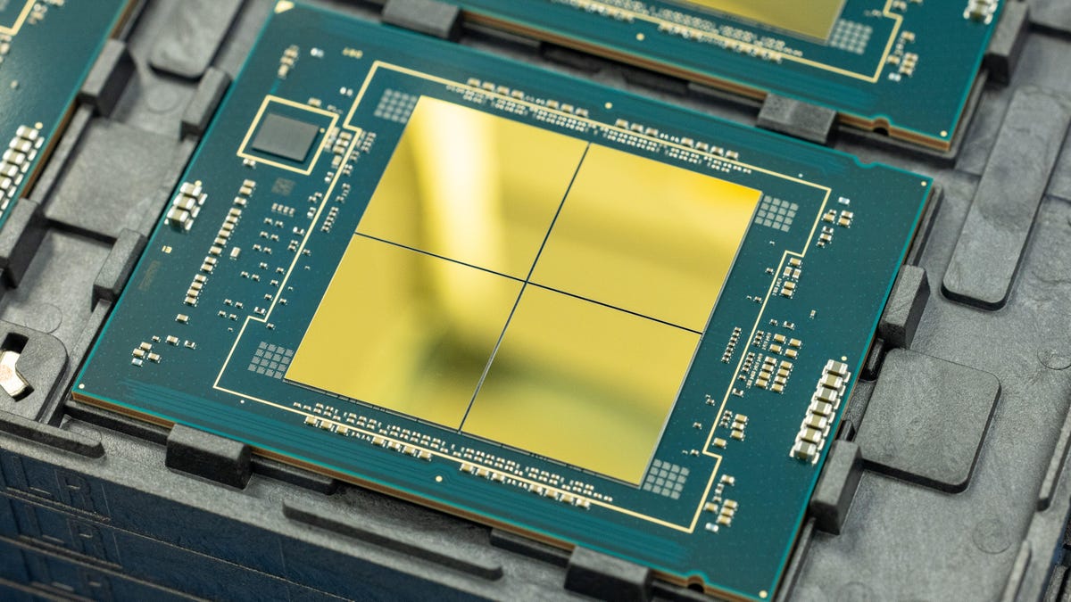
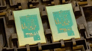
A real-world example of Intel's packaging technology is Intel's Sapphire Rapids, a large Xeon processor for data centers. Intel combines four CPU tiles, each also called a die or chiplet, into one larger processor. Intel's EMIB (embedded multidie interconnect bridge), a thin sliver of silicon underneath the edges where the tiles abut, supply data links across the processor so it behaves like one larger unit.
But in customer deals for packaging can lead to the deeper relationship that extends into chipmaking, in particular with the Intel 18A chipmaking process the company expects will surpass TSMC and Samsung in 2024.
"It's a foot in the door," Gardner said. "There's one customer in particular [for which] that trajectory of packaging first and advanced packaging then 18A is working well."
The power of packaging
Packaging is central to the Intel of today. Its newest Sapphire Rapids member of the Xeon server processor line uses a technology called an embedded multidie interconnect bridge, or EMIB, to link four chiplets into one large processor. A smaller chiplet (each also called a die) is less likely than a large one to be spoiled by a manufacturing defect, so manufacturing yields improve.
At Tuesday's Innovation event, Intel will shine a spotlight on Meteor Lake, its next-generation Core processor for PCs. It employs a different processor packaging technique called Foveros that stacks chiplets in three dimensions like pancakes -- and in Meteor Lake's case, most of the chiplets are Intel designs actually manufactured by its top rival, TSMC. Meteor Lake is expected to arrive in PCs later this year.
With those two products, along with more exotic processors like Ponte Vecchio, Intel has moved the bulk of its processor products to chiplet designs. In 2024, Intel plans to deliver more chiplet-based designs, including the big Granite Rapids and bigger Sierra Forest Xeon chips and the Arrow Lake PC chips expected in 2024.
Intel is the biggest fan of assembling "disaggregated" slices of silicon into bigger processors, but others have embraced it, too.
The M2 Ultra, the top-end Mac processor that completed Apple's two-year transition away from Intel chips, joins two M2 Max chips with a high-speed connection. And AMD, which relies on TSMC and Samsung to build its designs, has gained market share at Intel's expense with server chips that employ multiple chiplets.
It's unclear how much of the processor business will move from "monolithic," single-die designs to chiplet designs. There are still cost and simplicity advantages to avoiding advanced packaging. But it's clear the biggest processors -- the server and AI brains in data centers -- will become sprawling complexes of interlinked chiplets.
And that's where glass substrates should come in handy, with enough area, communication links and power delivery abilities to give chip designers room for growth.
"You start to hit your head on a technology," Feibus said, "and it's time to find a new way to do things."