At the Intel Photonics Lab in Santa Clara, Calif., researchers are pioneering new ways to transfer data at super fast rates using silicon germanium photodetectors.
Inside the labs, Intel is working to enhance the reliability of optical data transfer and seeking a diverse set of applications including supercomputing, data center communications, consumer electronics, automotive sensors, and medical diagnostics.
Mario Paniccia, director of the Photonics Technology Lab at Intel, took us inside the lab to look at some of the projects being pushed to market.
2 of 7 James Martin/CNET
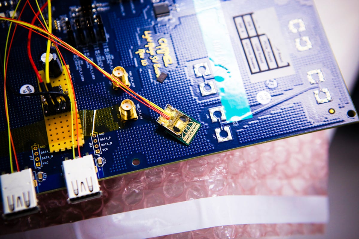
Optical USB
As Intel researches ways to develop integrated, high-volume silicon photonic chips, they are also looking for ways to deploy those new technologies into the marketplace, using photonics links for their systems and networks. Benefits can include extreme high-speed data transmission, like these optical USB ports, and may even have applications beyond digital communications, like expanding wireless networks by transporting analog RF signals and enabling lower-cost lasers for biomedical applications.
3 of 7 James Martin/CNET
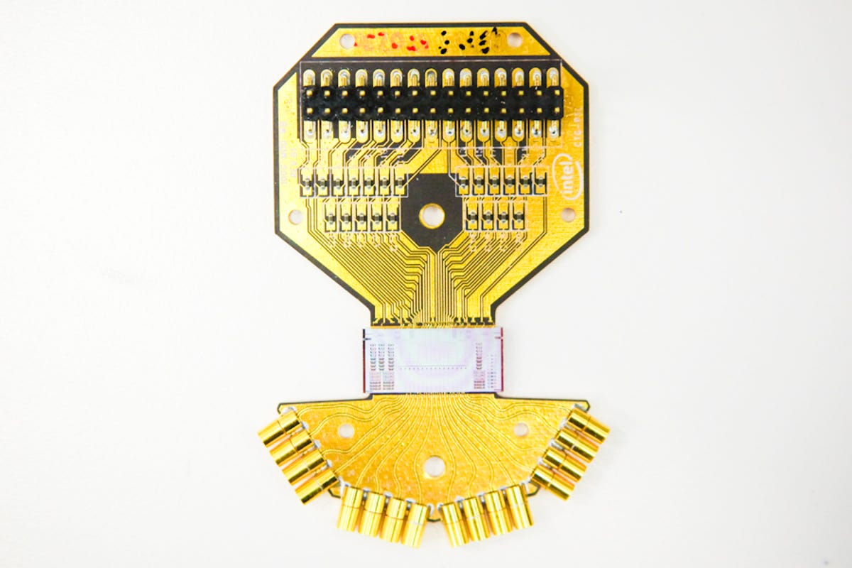
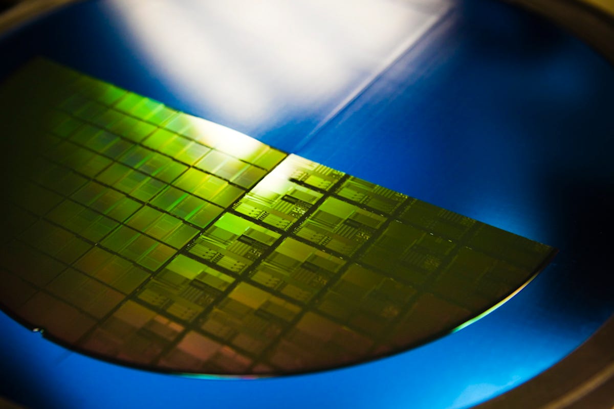
200 GB/s
In their work toward an integrated terabit optical chip, researchers at the photonics lab have created this chip capable of transmitting 200 gigabyte per second on eight channels of 25 GB/s each.
4 of 7 James Martin/CNET
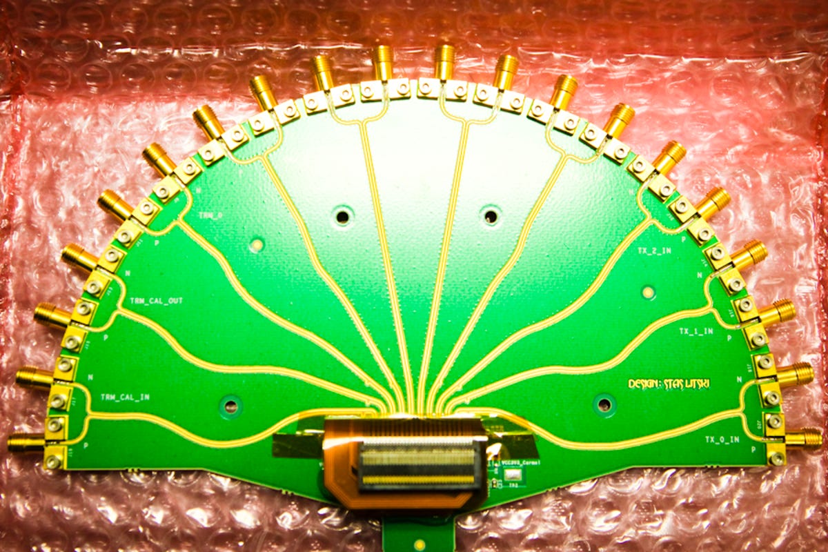
Silicon in photonics
Silicon has traditionally been used for electronics, providing more for less money, but Intel's researchers are exploring ways to do the same for photonics, using silicon technology to build optical devices that route, detect, and encode data.
5 of 7 James Martin/CNET
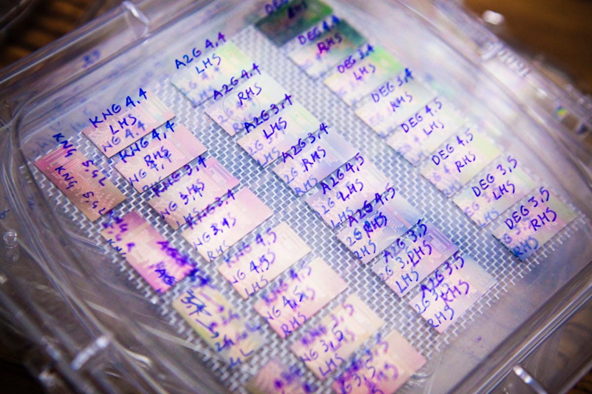
Photodetectors
Using silicon germanium photodetectors, Intel is taking optical data and converting the optical photons back into electrons, transmitting and receiving optical data in silicon, encoding data through the modulation of light.
6 of 7 James Martin/CNET
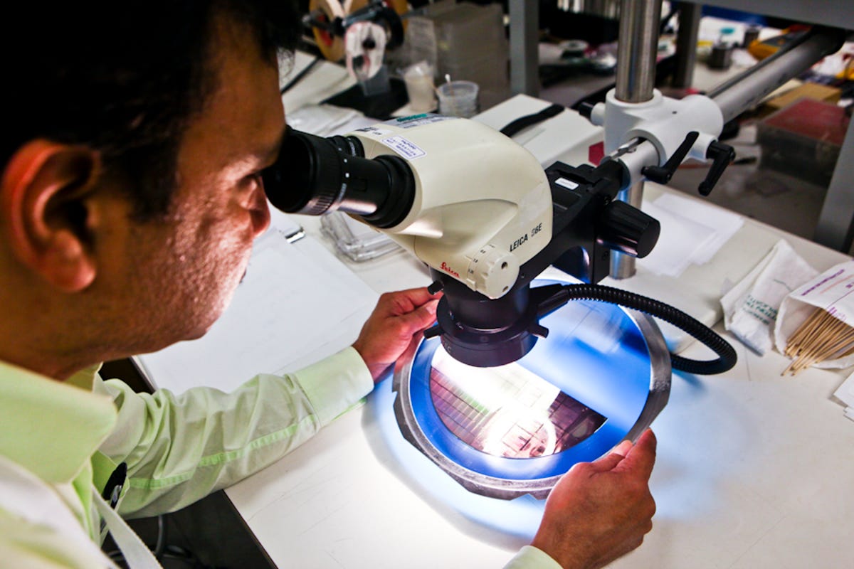
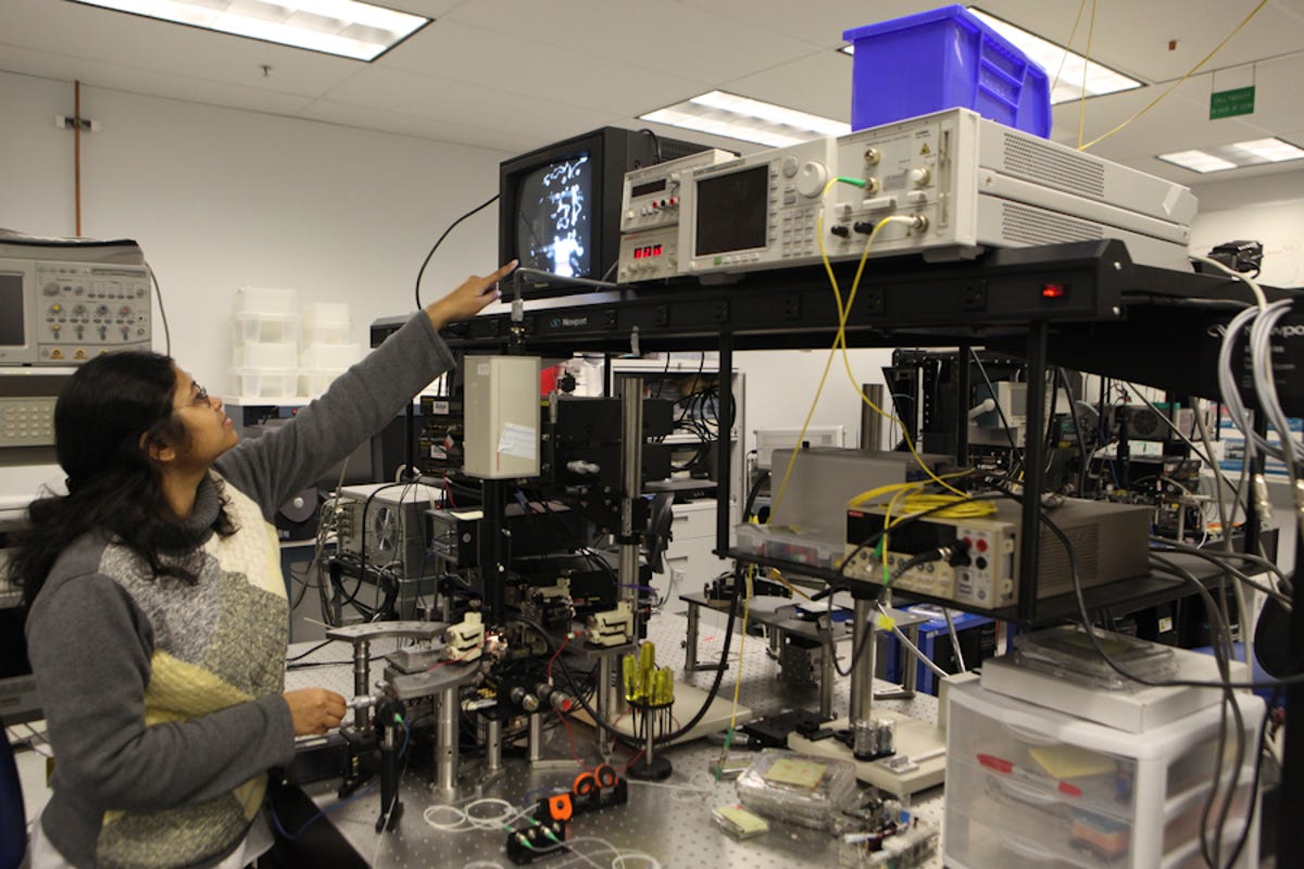
Researcher Juthika Basak
Researcher Juthika Basak at work inside one of the photonics labs at Intel in Santa Clara, Calif.
7 of 7 James Martin/CNET
Germanium silicon
Intel believes using germanium is important because, unlike silicon, it can efficiently detect light in the near infrared, which is the standard for communications. One of its drawbacks, however, is that so much stress is developed in pure germanium films deposited on silicon that defects are more likely within a germanium/silicon interface. At Intel's photonics labs, researchers are looking at different designs and processes that will minimize the impact of these defects on the electrical performance of the devices.