See Nvidia's H100 Hopper Chip Up Close
Exclusive: Here are the first detailed photos of the company's new flagship AI chip.


Nvidia H100 Hopper chip
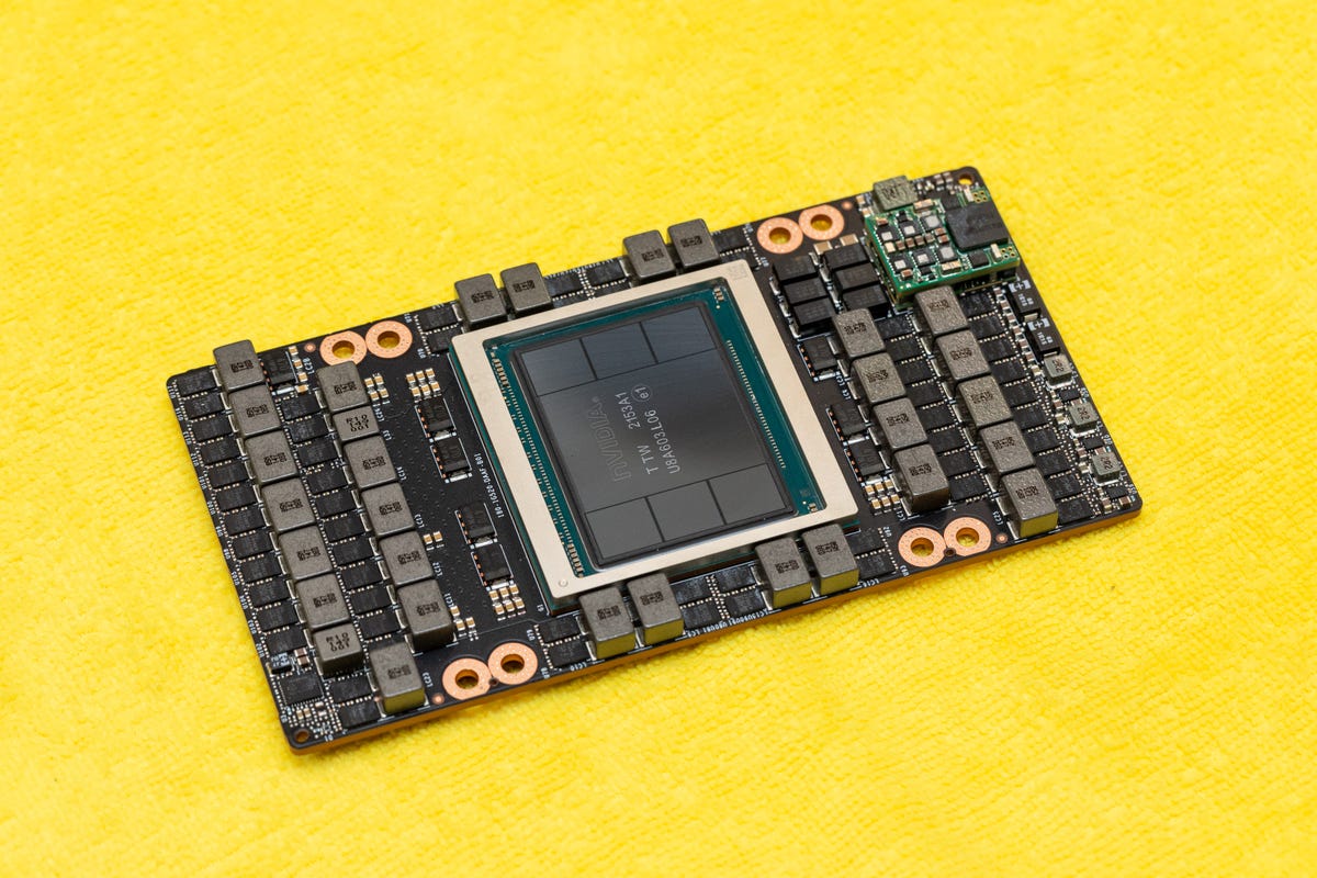
Nvidia's H100 "Hopper" is the next generation flagship for the company's data AI center processor products. It begins shipping in the third quarter of 2022. Here's a close-up look at the GPU, here shown mated to an electronics board studded with chunky power electronics.

Nvidia H100 Hopper chip
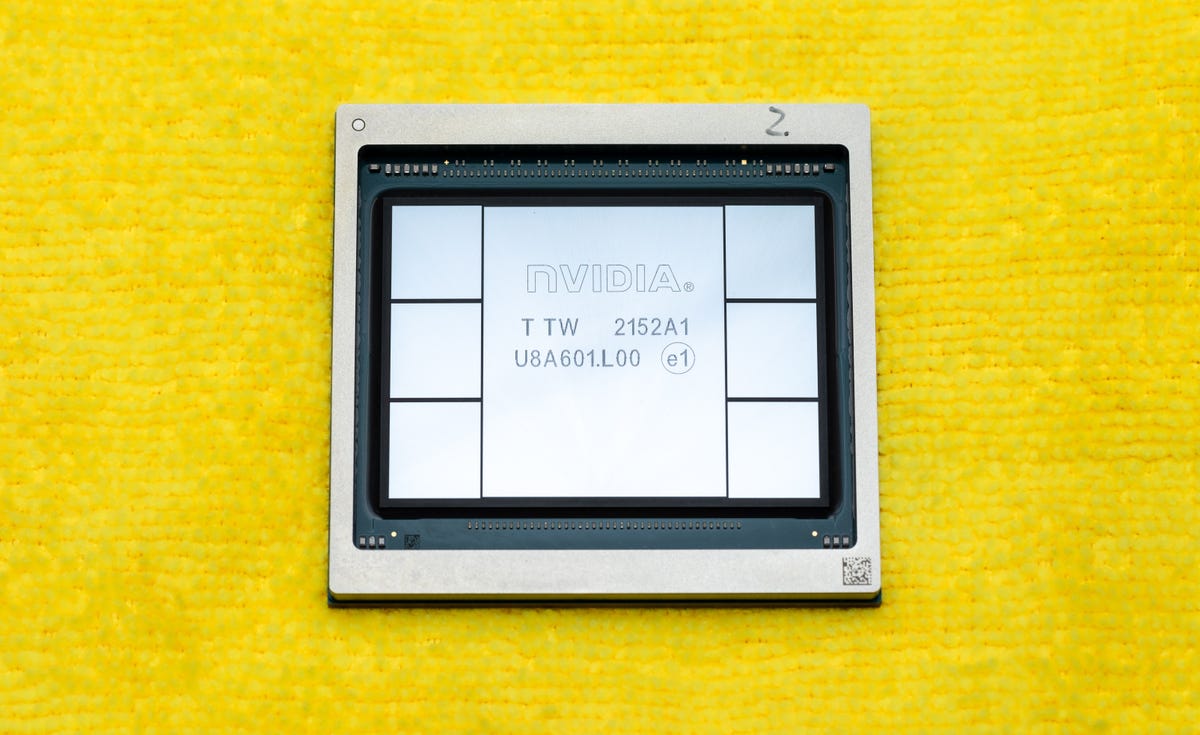
Nvidia's H100 "Hopper" processor is geared for artificial intelligence technology called machine learning. Overall, it's six times faster than the earlier A100, which arrived in 2020, Nvidia says. But that speedup will only apply for some customers, like those that can accommodate the H100's higher power consumption and adapt to the newer FP8 data format.

Nvidia H100 Hopper chip
Nvidia's H100 "Hopper" processor is particularly adapted to a newer AI processing approach called transformers. That's particularly important for natural language processing tasks like translating text or aiding software developers typing computer programs.
Nvidia H100 Hopper chip
One reason for Hopper's power is that the processor, mounted centrally in this package, is surrounded by a phalanx of high-bandwidth memory chips. AI models these days can require enormous amounts of memory, so fast access to up to 80GB of HBM speeds processing.
Nvidia H100 Hopper chip
Taiwan Semiconductor Manufacturing Co. (TSMC) builds Nvidia's H100 "Hopper" processor with its newer N4 process. The miniaturization let Nvidia cram 80 billion transistors into the processor's circuitry.
Nvidia H100 Hopper chip
The Hopper chip is a graphics processing unit descended from chips Nvidia has made for decades to speed up video games. But over the years, Nvidia has emphasized the processor lineage's mathematical and AI abilities, so calling it a GPU is something of a misnomer these days.

Nvidia H100 Hopper Chip Compared to a Pocketknife
Nvidia's H100 "Hopper" processor isn't big compared with a pocketknife, but at 814 square millimeters, it's just about as big as a single chip can be with today's chipmaking equipment. Large sizes mean steep prices, but H100 predecessors like the A100 from 2020 have sold well, and that chip is fractionally larger.
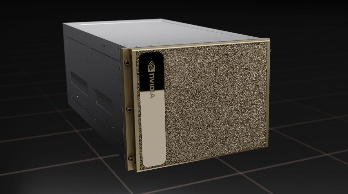
Nvidia DGX H100 System
Nvidia's DGX H100 System houses eight Hopper GPUs in a chunky, rack-mountable chassis. The H100 processors can be linked with the high-speed NVLink connections to share a single pool of memory.

Nvidia DGX H100 Superpod
Connecting 32 Nvidia's DGX H100 systems results in a huge 256-Hopper DGX H100 Superpod. They all H100 are linked with the high-speed NVLink technology to share a single pool of memory. Customers like Facebook and Tesla that buy this much GPU horsepower are relatively rare.
More Galleries

My Favorite Shots From the Galaxy S24 Ultra's Camera
20 Photos
Honor's Magic V2 Foldable Is Lighter Than Samsung's Galaxy S24 Ultra
10 Photos
The Samsung Galaxy S24 and S24 Plus Looks Sweet in Aluminum
23 Photos
Samsung's Galaxy S24 Ultra Now Has a Titanium Design
23 Photos
I Took 600+ Photos With the iPhone 15 Pro and Pro Max. Look at My Favorites
34 Photos