Exploring nanomaterials for a solar breakthrough (photos)
MIT and oil company Eni open the doors to the Eni-MIT Solar Frontiers Research Center, where researchers are experimenting with materials and equipment for low-cost solar.


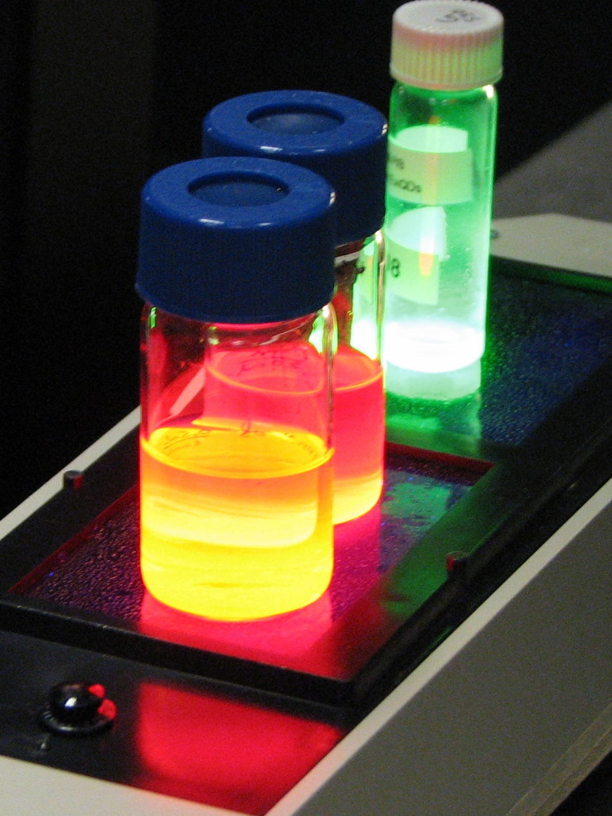
Solar cell in a bottle
CAMBRIDGE, Mass.--If things play out as hoped, these vials hold the seeds for future solar cells.
Inside are quantum dots, crystals that are only a few nanometers in size, made from carbon-based dyes. It's one of the avenues of research at the Eni-MIT Solar Frontiers Research Center, which was officially dedicated on Tuesday.
Researchers are working at the molecular or quantum dot level, which allows them to fine-tune the light-absorption properties and band gap of the semiconductor materials, explained Vladimir Bulovic, the director of the center, during a tour on Tuesday.
Thin-film solar cells made from quantum dots have the potential to dramatically lower the cost of solar power and enhance traditional silicon solar panels. But it will take years before they become commercially viable. It typically takes 10 years between invention and commercialization and these technologies are still in their early years.
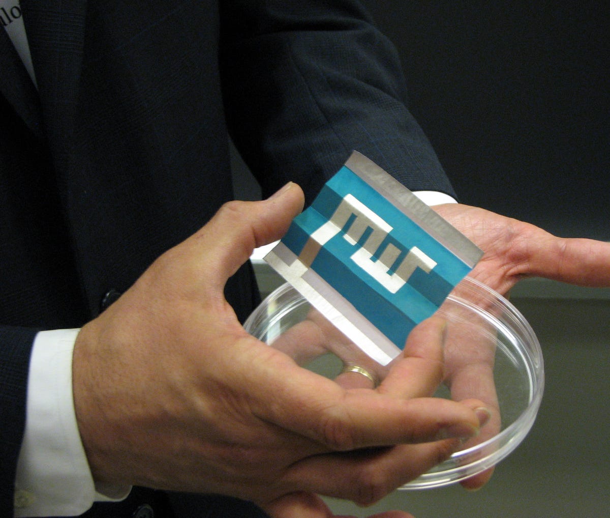
Printing solar cells on paper
Using nanoscale materials means that solar cells can be deposited onto a wide range of substrates, including flexible plastic and metal foils. MIT researchers claim to be the first to coat paper with the two layers of semiconductor needed to make a solar cell. In this case, they used a carbon-based dye but the breakthrough was the coating process, which is similar to an inkjet printer, explained Bulovic.
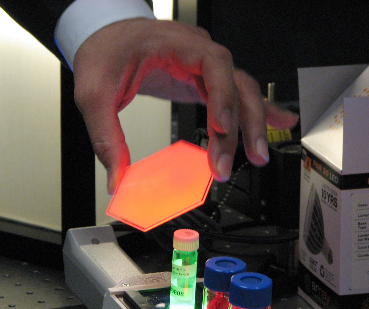
Making light with quantum dots
Already, scientists can generate light from quantum dots, but making a photovoltaic cell that can create a current of electricity is much harder. Here Bulovic shows a thin-film material that lights up in the presence of ultraviolet light.
The box on the table to the right is an example of an LED light made with similar technology. Array Lighting is releasing this year an LED with an Edison screw, which uses 80 percent less energy than comparable incandescent lights. The quality of the light is also comparable to incandescents, said Bulovic.
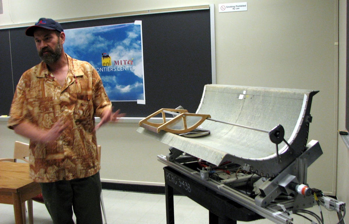
Reflective trough made from auto parts
Massachusetts Institute of Technology mechanical engineering professor Alex Slocum shows off a prototype of a reflective trough designed and being tested at MIT.
Parabolic troughs are a mainstay of large-scale concentrating solar power systems, which concentrate sunlight to make heat or squeeze more electricity from photovoltaic solar cells. The problem that troughs pose is that they accumulate dirt, which decreases their reflectivity, and they typically need to be placed on a terrain that is long and flat.
The prototype shown by Slocum, which is about one-tenth the scale of a commercial trough, is designed for low cost and modularity. The goal is to make it small enough so that auto industry parts can be used for the mechanisms that move the trough to follow the sun. Researchers also added a lip to the edge of the trough so that when heavy winds come, it will cause a vibration that will move the accumulated dirt, he explained.
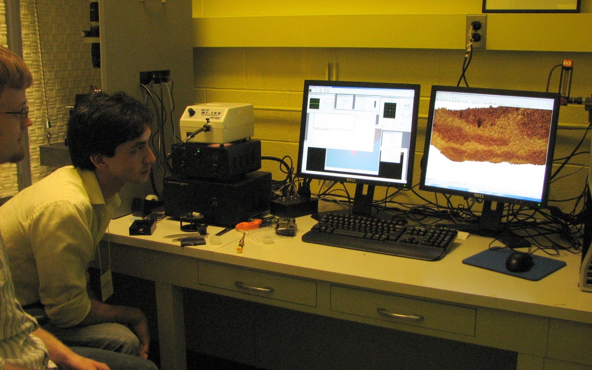
Inspecting on the nanoscale
MIT students in the Eni-MIT Solar Frontiers Research Center watch a computer visualization of the texture of a nanomaterial. Seeing the physical surface of materials, such as quantum dots, provides clues for researchers seeking cheap solar cells. For example, this image shows that there is a definite structure to the specimen, which could indicate it can self-assemble into a desirable shape.
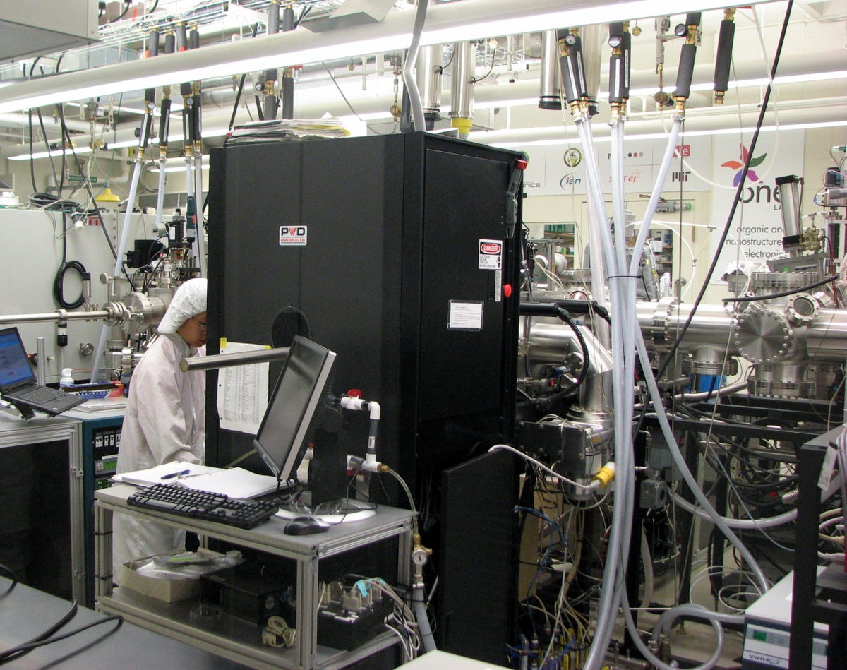
Materials growth system
One of the key pieces of equipment in the solar lab at MIT is what Bulovic called "an integrated materials growth system for nanostructured thin films." With it, researchers can test various fabrication techniques for depositing layers of semiconductor material, including vapor deposition, sputter deposition, and printing. The speed and efficiency of the manufacturing process for thin-film solar cells is vital to keeping the costs down.
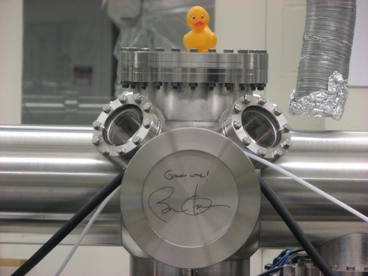
Obama stops by
When President Obama came to MIT last October, he visited various clean-energy research projects including this solar lab, which is funded in part by the National Science Foundation. This piece of equipment, seen in full in the previous picture, is for testing different processes for depositing nanomaterials. Above Obama's signature, it says "Great work!"
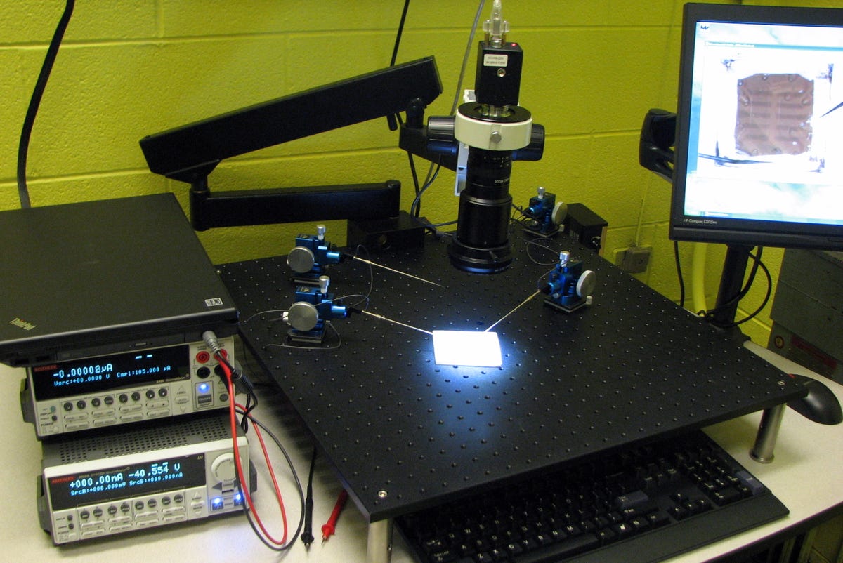
Ten in a row
Another scene from the solar research lab. This is an experiment with placing 10 solar cells on an organic thin-film.
More Galleries

My Favorite Shots From the Galaxy S24 Ultra's Camera
20 Photos
Honor's Magic V2 Foldable Is Lighter Than Samsung's Galaxy S24 Ultra
10 Photos
The Samsung Galaxy S24 and S24 Plus Looks Sweet in Aluminum
23 Photos
Samsung's Galaxy S24 Ultra Now Has a Titanium Design
23 Photos
I Took 600+ Photos With the iPhone 15 Pro and Pro Max. Look at My Favorites
34 Photos