Intel touts multiscreen flexibility with 'display as a service'
By hooking displays to a network, users can send video from their devices to any available screen.


- Shankland covered the tech industry for more than 25 years and was a science writer for five years before that. He has deep expertise in microprocessors, digital photography, computer hardware and software, internet standards, web technology, and more.
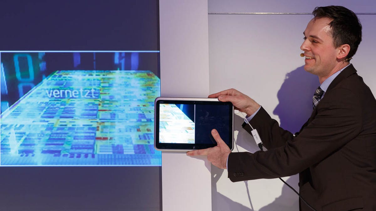
HANOVER, Germany--Intel today debuted a technology called display as a service (DAAS) that it hopes will transform how people use their gadgets.
The technology breaks the hard link between a video source and a screen the way virtualization software breaks the hard link between an operating system and a processor. With DAAS, people can view what's on their tablet on a big-screen TV, mirror the same imagery on multiple displays, or link up multiple displays to create a single, bigger display.
Another possibility, which Intel Labs' Divya Kolar described on blog post, is to combine multiple devices' video onto a single screen so a whole family can work together on multiple projects.
With DAAS, each display becomes a bunch of pixels available for any device to use. Image data is sent over a wired or wireless network.
Intel announced and demonstrated the technology here at the CeBIT trade show. It also showed off a small box that can bring the technology to displays that don't have the requisite IP address.

Also at CeBIT, Intel showed off a prototype Windows 8 laptop, built with its upcoming fourth-generation Core processor, called Haswell. The laptop prototype -- one of only four in the world -- has a screen that can be detached with one hand.
Haswell, due to arrive in systems midyear, is built on the same manufacturing process as today's Ivy Bridge processors, but it will introduce a new microarchitecture. Intel has been mum on the details beyond promising better power management, but expect better graphics performance and somewhat faster processing.
Later this year, Intel will release the earliest chips, called Broadwell, that shrink the Haswell design using the next-generation manufacturing process. Broadwell chips measure 14 nanometers (billionths of a meter), down from 22nm in Ivy Bridge and Haswell chips.

"We're going to be introducing the 14-nanometer technology at the end of this year and [will] start ramping it next year," said Christian Morales, general manager of Intel's operations in Europe, the Middle East, and Africa.
Also coming will be a new manufacturing process that shifts to silicon wafers measuring 450mm across rather than today's 300mm. The larger wafers lower the per-chip cost of manufacturing because more processors can fit onto a single wafer.
The transition is tremendously expensive, though, because new manufacturing equipment is required. It's one reason Intel has been increasing its capital expenditures, Morales said.
"We want to go into 450mm wafers in the very near future," Morales said.