Samsung's next-gen chip technology delayed until 2022
The company's 3-nanometer manufacturing technology is late, but its more advanced 2nm successor will arrive in 2025.


- Shankland covered the tech industry for more than 25 years and was a science writer for five years before that. He has deep expertise in microprocessors, digital photography, computer hardware and software, internet standards, web technology, and more.
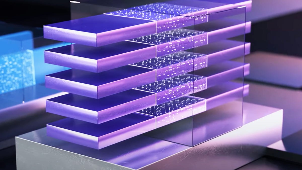
Samsung's gate-all-around transistor design, where shown here with purple conductors penetrating a transparent surrounding gate material, is due to arrive in processors in 2022.
Samsung, one of the three leading edge processor manufacturers, had planned to start building a faster and more efficient class of chips in 2021, but instead the new design will instead arrive in the first half of 2022. The Korean electronics giant shared the schedule for the shift during its Samsung Foundry Forum on Wednesday.
The slip means customers that rely on Samsung will have to wait longer to tap into the leading-edge technology. Among the biggest names using the company's services are phone chip designer Qualcomm, server maker IBM and Samsung itself.
The good news for those customers, though, is that Samsung also announced progress in the next generation of manufacturing afterward, a refinement that should arrive in the second half of 2025. That should deliver another step forward in chip performance, power efficiency and electronics miniaturization, Samsung said.
Samsung's top chipmaking rival, Taiwan Semiconductor Manufacturing Co., disclosed a delay to similar technology in August. The schedule slips ease the pressure a little on Intel, which is launching its own foundry business as part of a recovery plan aimed at reclaiming the leadership it lost to TSMC and Samsung.
The processor business is under extreme pressure. With the pandemic boosting PC sales, smartphone usage, and online services run out of data centers, demand for processors has outstripped manufacturing capacity. The chip shortage has hobbled sales of PCs, game consoles, cars and other products reliant on world-spanning electronics supply chains.
Based on Samsung's conversations with customers, the processor shortage won't ease until 2022, said Shawn Han, a Samsung Foundry corporate senior vice president, based on Samsung's conversations with customers. "From our view, it will be lasting another six to nine months, although we are investing, and other foundries suppliers are increasing their capacity," he said in a briefing ahead of the Samsung Foundry Forum.
Moving to next-generation manufacturing technology is extraordinarily complicated. Chips are made of billions of electronic components called transistors, each vastly smaller than a speck of dust. Chip fabrication plants, called fabs, etch the circuitry patterns on silicon wafers with a process requiring dozens of steps that take months.
Progress comes by miniaturizing transistors so more can be squeezed onto a chip, increasing their speed and decreasing their power consumption. Samsung's next-gen process, which it calls 3GAE, employs a technique called gate all around (GAA). It's an early version of the technology.
In 2023, Samsung expects to reach high production volume with a more mature version called 3GAP. The 3 in the name refers to the 3-nanometer measurement that, although no longer directly linked to the dimensions of chip electronics, serves as a label for progress in manufacturing methods.
2 nanometer manufacturing in 2025
Then in 2025, the company plans to move to a second, more advanced gate-all-around technology it calls 2GAP. That manufacturing method will be the first of Samsung's 2nm generation. One improvement will be in the number of current carrying "nanoribbons" that will penetrate the surrounding gate material, which will increase from 3 in the 3nm generation to 4 nanoribbons.
As chips get more complex, they also often get more expensive, which is why many chip buyers are sticking with older, cheaper manufacturing processes from companies like GlobalFoundries.
But Samsung believes it can make the new manufacturing processes financially alluring to customers.
"Even though GAA is a difficult technology, We will still strive to lower the cost per transistor," said Moonsoo Kang, head of Samsung's Foundry Strategy Team. "That trend will continue."
Chip packaging improvements
For decades, Moore's Law has charted how miniaturization has let chip designers pack more and more transistors into a given chip area. But the slowing pace off miniaturization has made other avenues of progress more important.
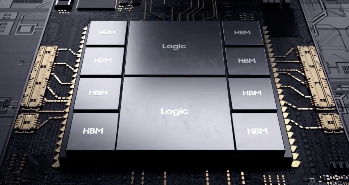
Samsung chip packaging technology will let it join eight high-bandwidth memory chips with two central processors in a future design called I-Cube8.
One key direction is packaging -- the ways different "chiplets" can be connected into one larger processor. Samsung is working to improve the variety of chips that can be connected edge to edge, called a 2.5D integrated circuit, or sandwiched on top of eachother, called 3D. It's also working on packing data links between the chips more densely for higher speed connections.
And it's got a new term for the combination of 2.5D and 3D connections: 3.5D. "This kind of chip will allow us to achieve unprecedented performance and density," Kang said in a talk.
That's what Intel already is doing with its Ponte Vecchio processor, an exotic chip good for graphics, artificial intelligence and supercomputing purposes.
One big advantage of the packaging advances is an idea called heterogeneous integration -- combining a wide variety of chips built with different processes. That lets chipmakers merge expensive older manufacturing processes for some components and cutting-edge processes for parts where performance is critical, for example.