The chip industry is intensely focused on steady improvements to processor cost and performance. Here's a look at some of technology involved in building today's chips and researching tomorrow's.
Stephen Shankland
Stephen Shankland worked at CNET from 1998 to 2024 and wrote about processors, digital photography, AI, quantum computing, computer science, materials science, supercomputers, drones, browsers, 3D printing, USB, and new computing technology in general. He has a soft spot in his heart for standards groups and I/O interfaces. His first big scoop was about radioactive cat poop.
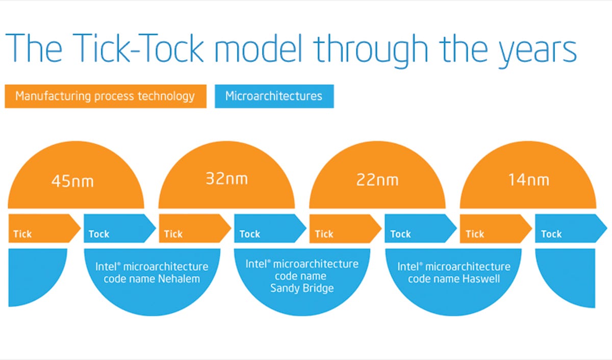
With Intel's "tick-tock" approach, it moves to a new chip manufacturing technology every two years -- the cadence Moore's Law dictates. On the years in between, Intel updates the chip architecture but leaves the manufacturing process unchanged.
2 of 21 Intel
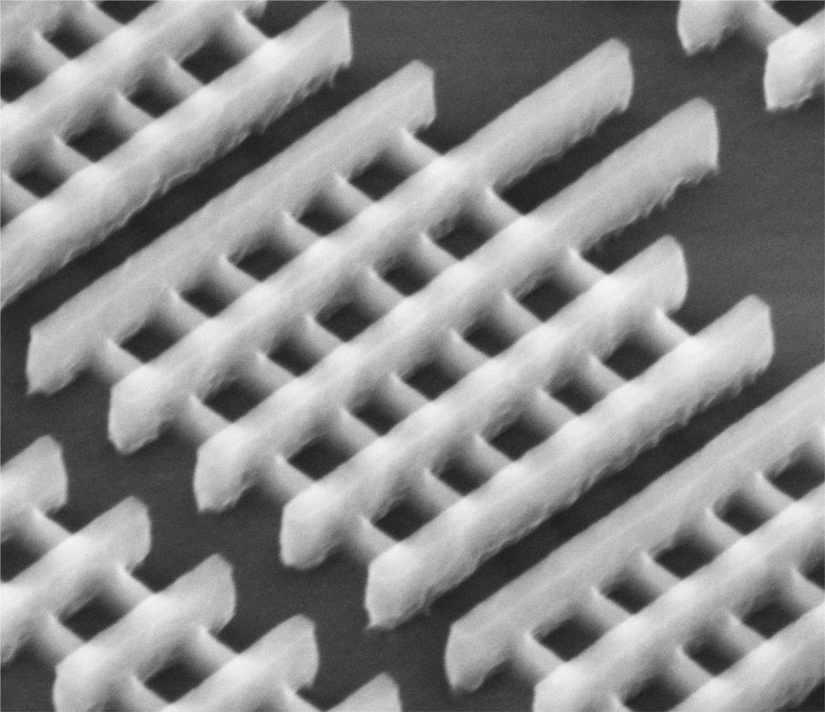
Intel's 22nm tri-gate transistors
To shrink its microprocessor circuit elements to the 22-nanometer size -- just 22 billionths of a meter -- Intel had to develop a technology called tri-gate transistors. Transistors are tiny switches, with a gate on top controlling whether electrical current flows through a silicon channel underneath. The big innovation for 22nm manufacturing is that the channels are now fins that protrude out of the plane of the silicon chip. Previously they lay flat within the chip. In this photo of the 3D "tri-gate" design, the gates are the taller ridges going up and to the right, and the fins are the somewhat lower ridges going up and to the left. A single transistor can have multiple fins going underneath a single gate.
3 of 21 Intel
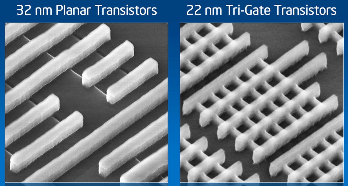
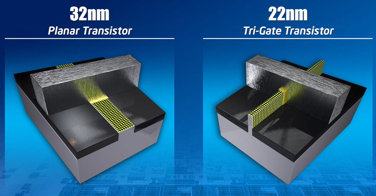
Intel 32nm vs 22nm chip manufacturing
This view compares the last-generation 32nm process used to make Intel's "Sandy Bridge" chips with today's 22nm process for "Ivy Bridge" chips. Where the 22nm chips have protruding fins to channel electrical current, the 32nm design uses a traditional "planar" design where the channel is flat within the chip surface.
4 of 21 Intel
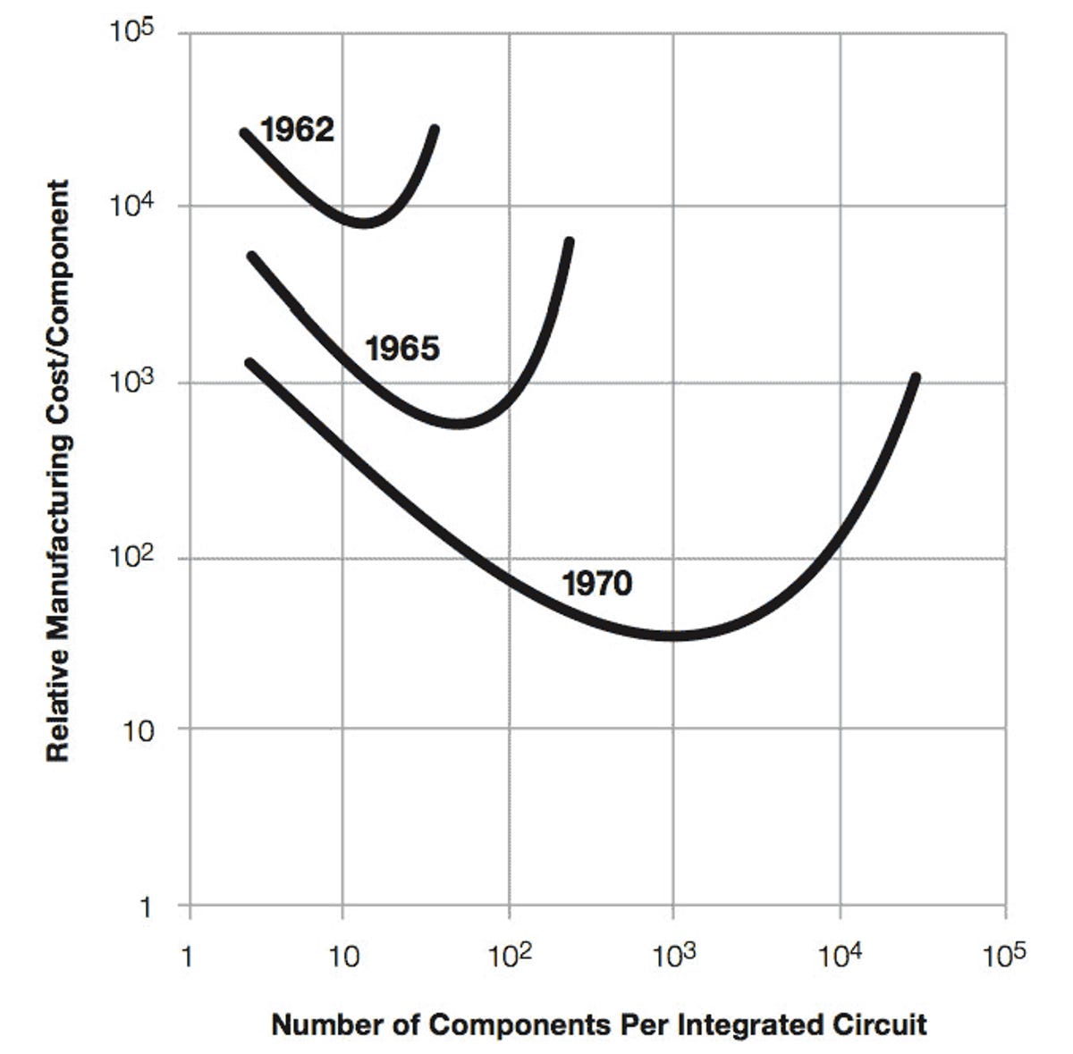
The original Moore's Law chart
This chart from Intel co-founder Gordon Moore's seminal 1965 paper showed the cost of transistors decreased with new manufacturing processes even as the number of transistors on a chip increased.
5 of 21 Intel
Planar vs 3D transistors
This computer diagram shows the change from the planar transistors on the left, where the silicon channel is within the plane of the processor, and "tri-gate" transistors, also known as 3D or finfet transistors because the channel protrudes like a fin. (FET stands for field effect transistor.) Intel went to tri-gate designs for its 22nm manufacturing process.
6 of 21 Stephen Shankland/CNET
Intel co-founder Gordon Moore
Intel co-founder Gordon Moore, shown here speaking in 2007 at the Intel Developer Forum in San Francisco, wrote the papers in 1965 and 1975 that described what later became known as Moore's Law.
7 of 21 National Academy of Sciences
Chip frequency scaling hits a wall
A National Academy of Sciences report shows how processor clock speeds, measured here in megahertz, aren't increasing at the pace they had for years earlier.
8 of 21 Mears Technologies
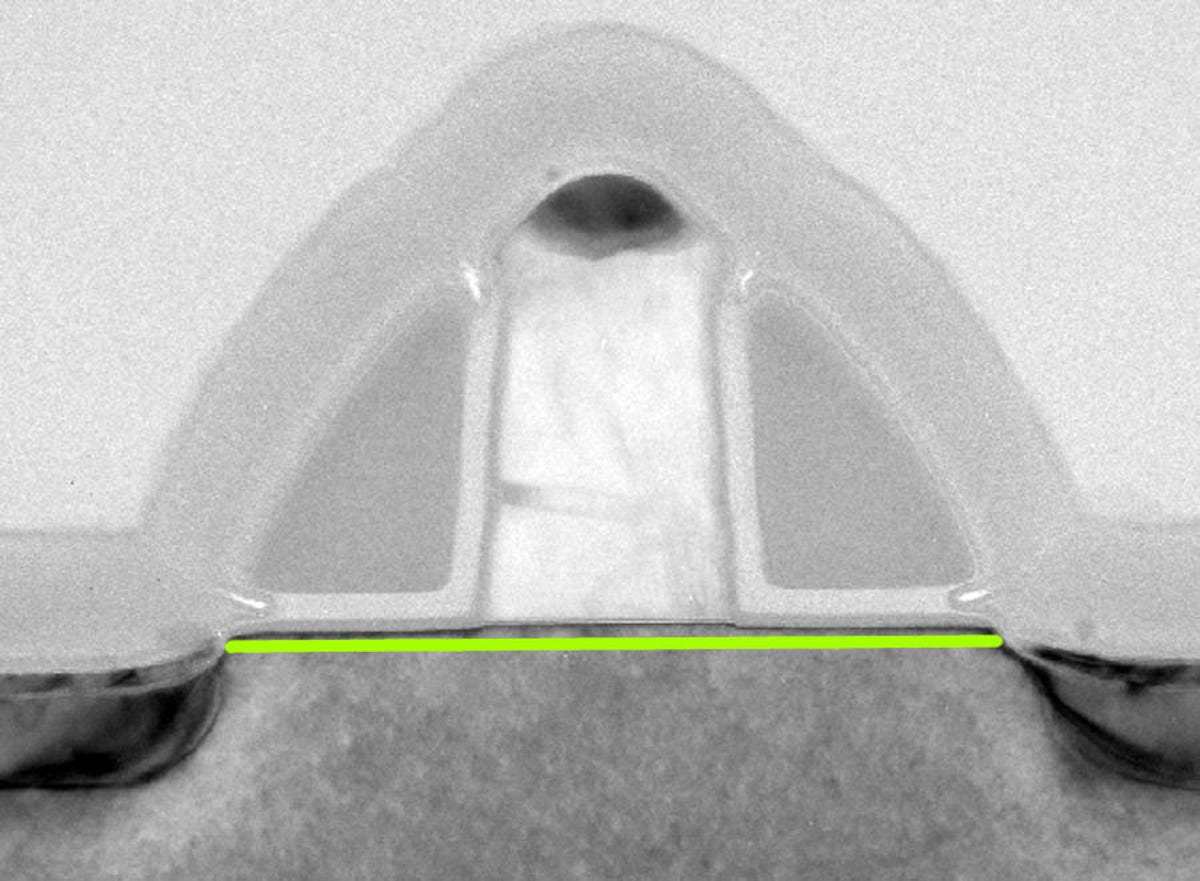
Mears' silicon methods
Mears Technologies hopes its transistor technology will extend the lifespan of traditional silicon transistors, the tiny semiconductor switches at the heart of microprocessors. This cross section of a transistor shows the gate across the top that controls whether current flows in a silicon channel, the darker source and drain areas on either end of the current pathway, and an area marked in green area where Mears' MST technology is added. The MST technology gives more precise control over elements added to the silicon channel, a process Mears says reduces variability so smaller transistors that consume less power are practical.
9 of 21 IBM
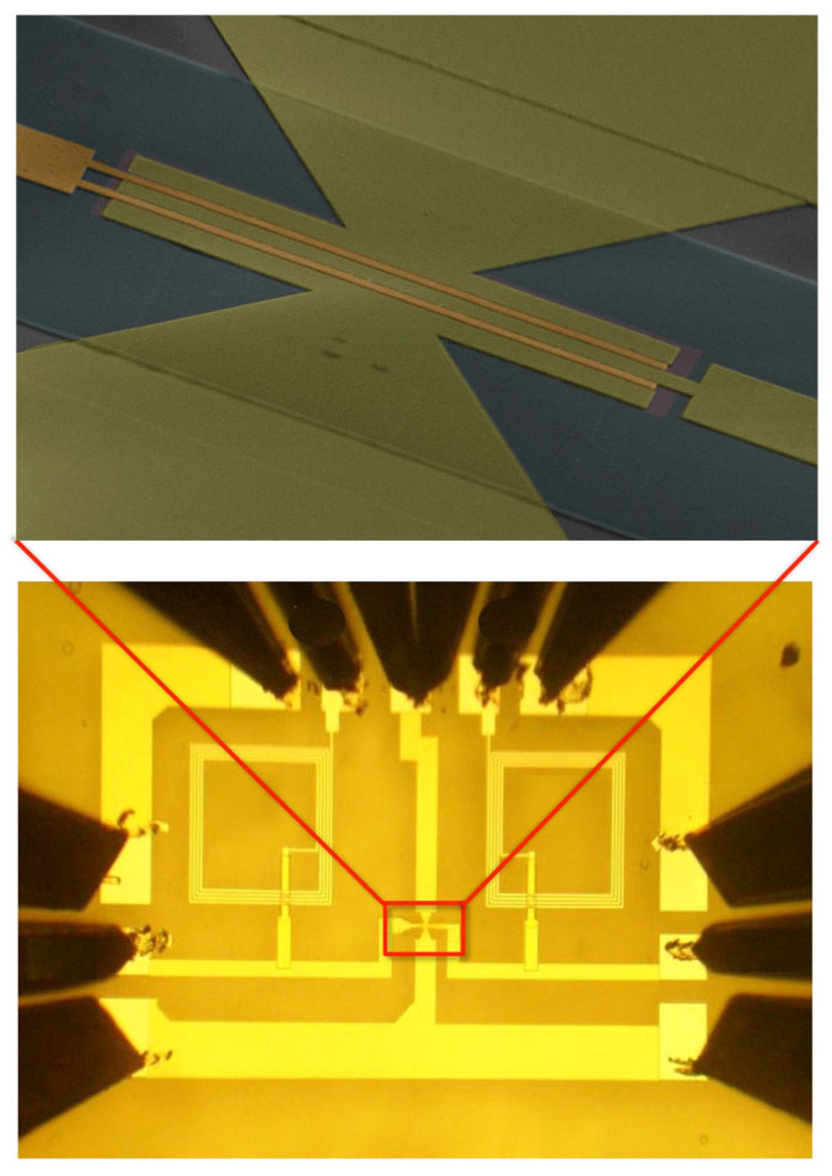
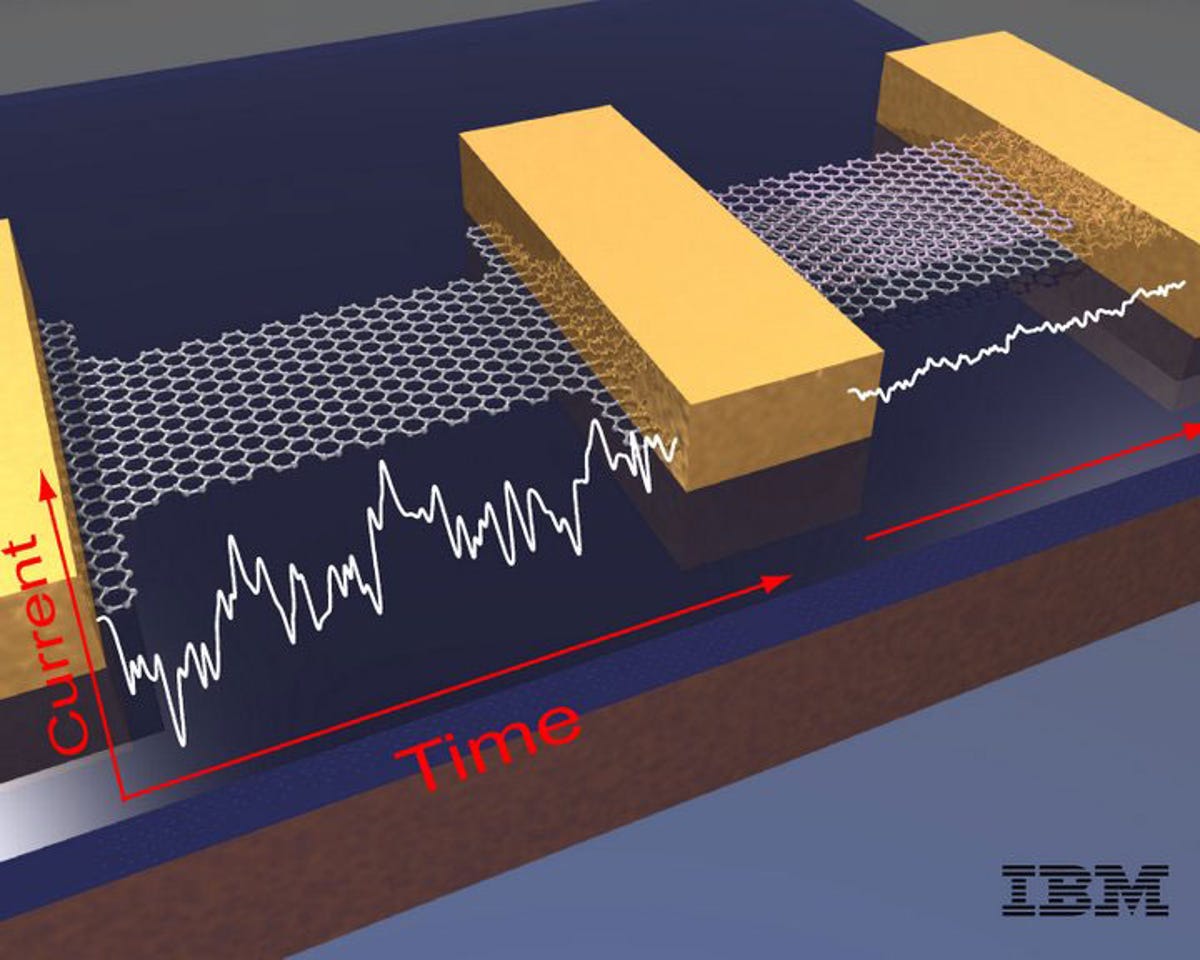
IBM graphene transistor integrated circuit
IBM has figured out how to build a graphene-based transistor on an integrated circuit geared for wireless communication purposes, not for computing.
10 of 21 Intel
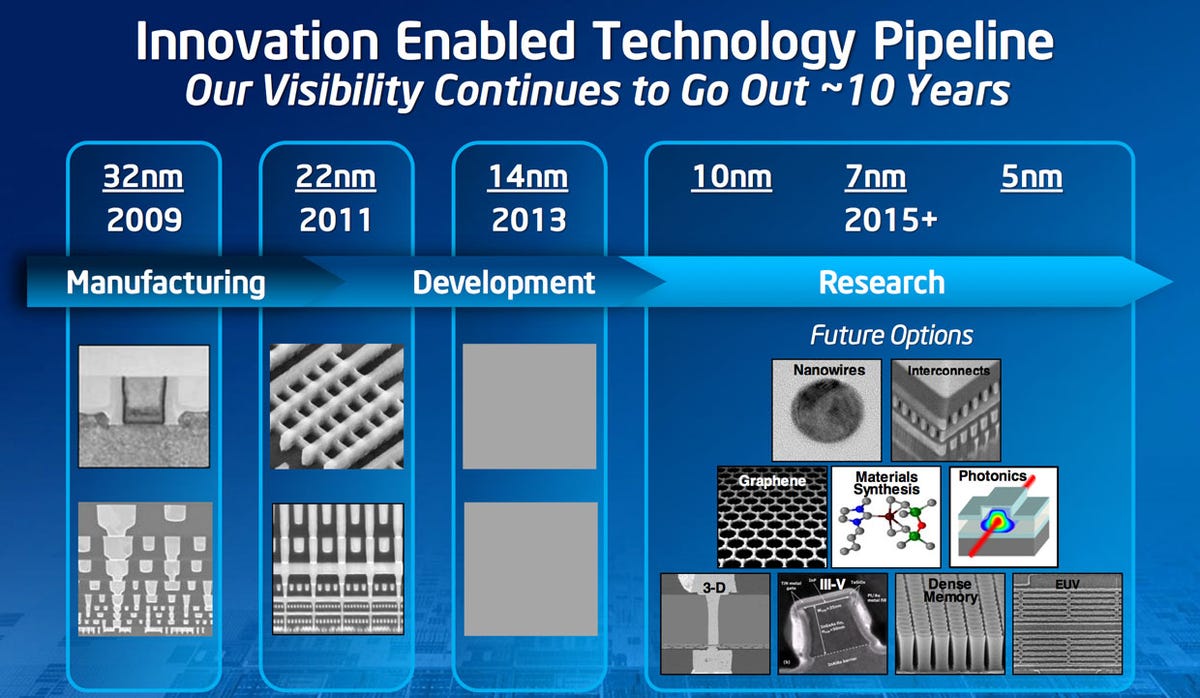
Looking into future chip technology
Staying on the Moore's Law treadmill involves tackling a constant series of technical challenges. Intel has maintained an ability to predict what will happen for about the next decade.
11 of 21 IBM
Carbon nanotube
It's getting harder and harder to build transistors with silicon semiconductor channels. One alternative IBM is pursuing are transistor channels made of carbon nanotubes, a lattice of carbon atoms rolled into a tube.
12 of 21 Intel
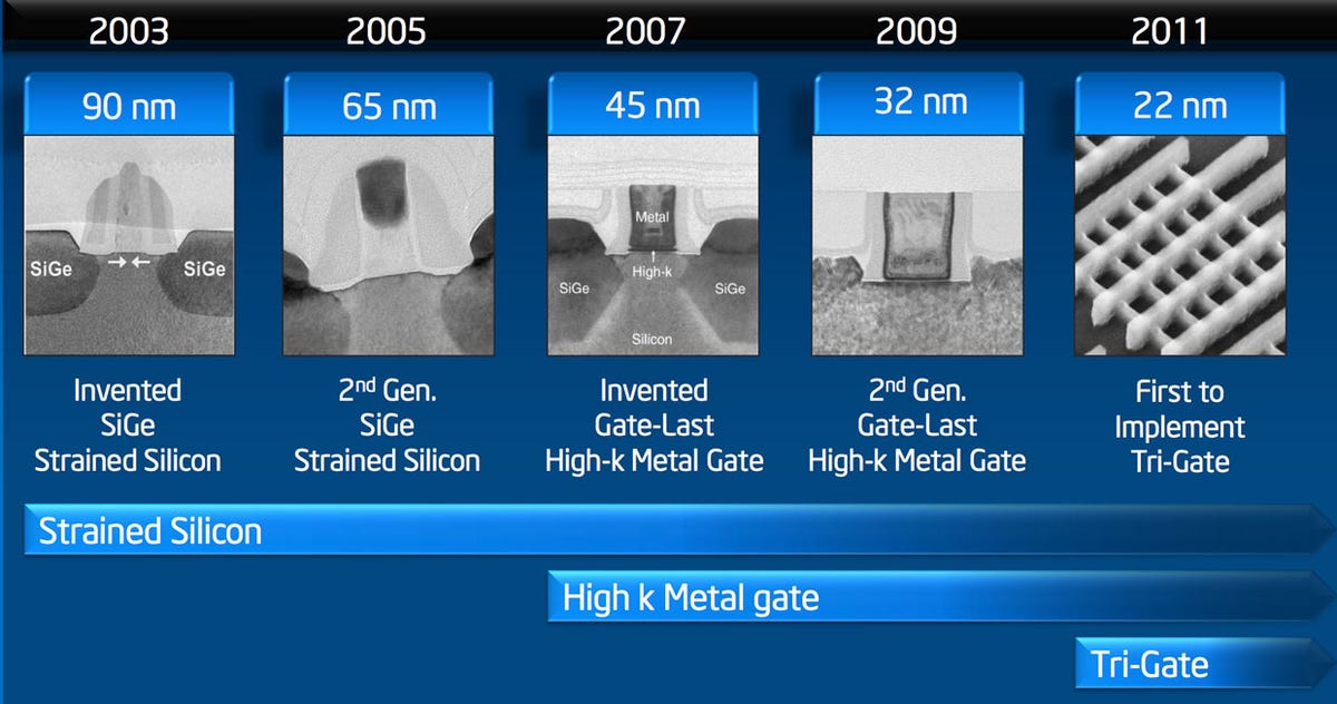
Keeping Moore's Law ticking
Intel, which gears its manufacturing changes to Moore's Law, introduces a new process every two years. This diagram shows some of the major innovations that let it keep pace. After moving from a 90nm manufacturing process in 2003 to the 22nm process used to make today's "Ivy Bridge" chips, Intel can pack about 16 times as many transistors into a same-sized chip.
13 of 21 Intel
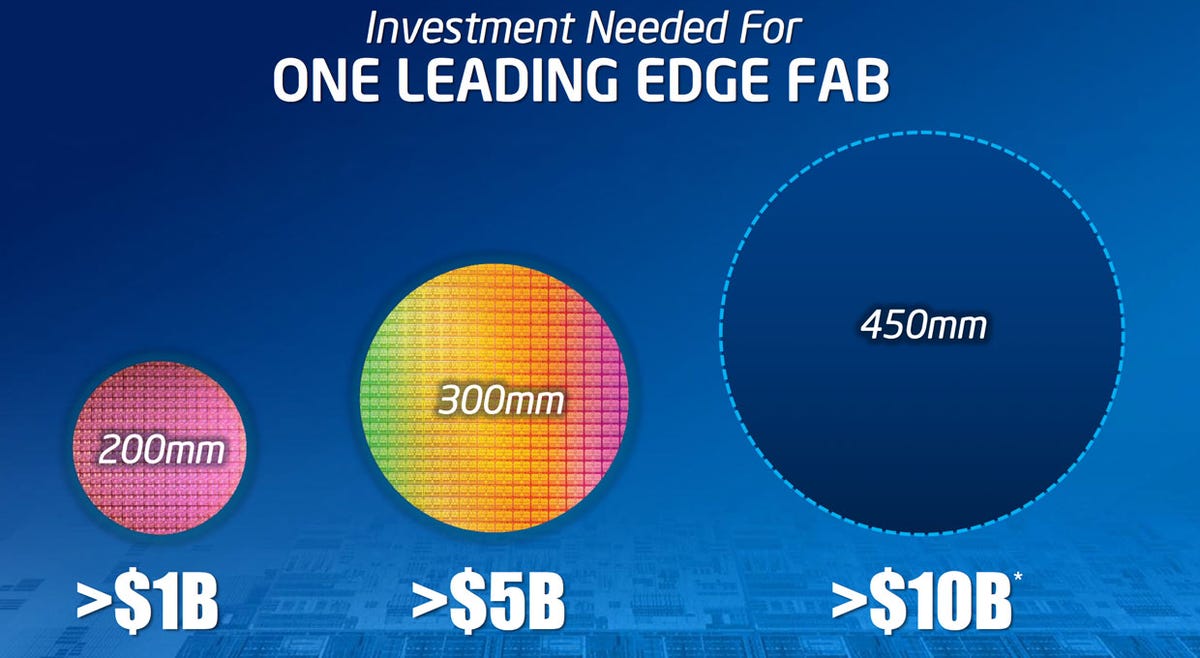
Fab costs increase
The cost of building a "fab" -- a chip fabrication plant -- has been getting steadily more expensive for new generations of processors and for using larger silicon wafers. Each circular wafer is carved into many chips, and using larger ones lowers per-chip costs. But building the fab is more expensive -- Intel expects future fabs that handle 450mm wafers will cost $10 billion each.
14 of 21 Intel
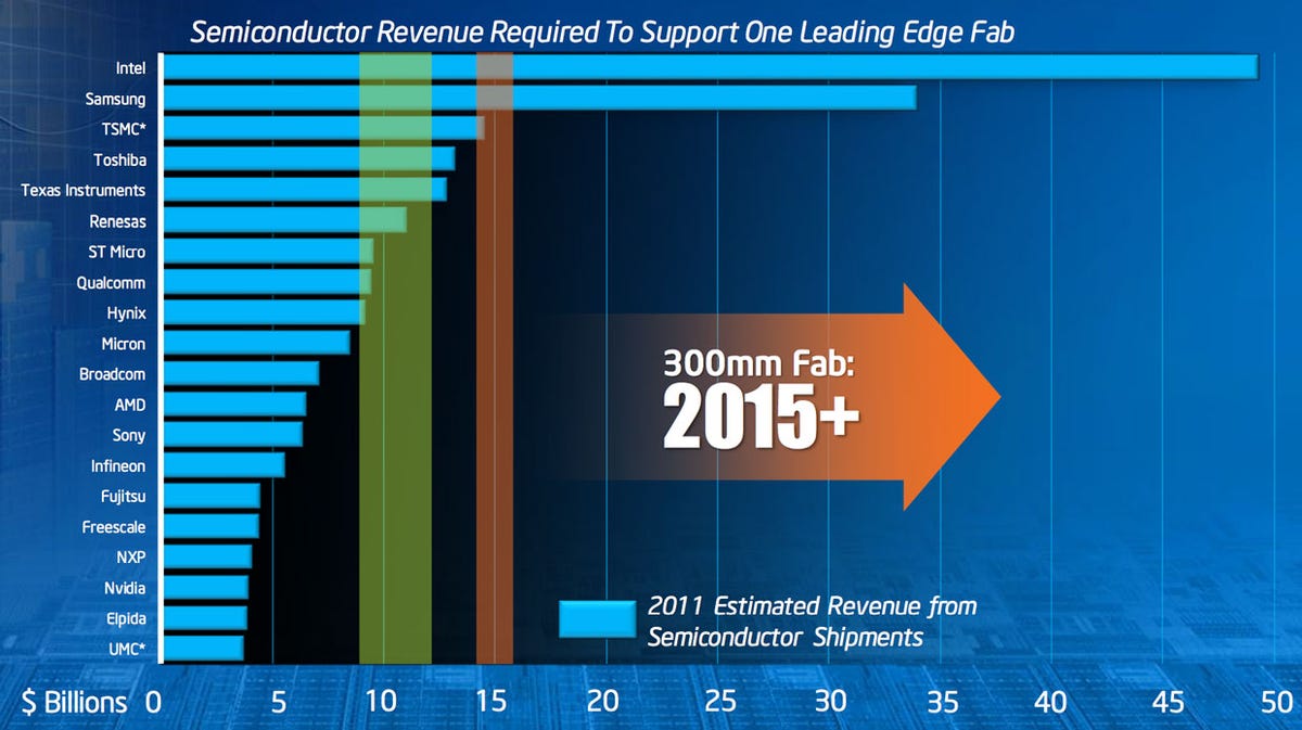
Prohibitive fab costs
As chip factories ("fabs") get more expensive to build, fewer companies can afford them. In this Intel chart, the green band shows the companies that can afford to build a fab that makes chips out of 300mm silicon wafers. The orange band shows the much smaller number that can afford to build chips with a 2015 manufacturing process. (The chart is based on the companies' 2011 chip revenue and a profitability assumption of 40 to 50 percent gross margins.)
15 of 21 Intel
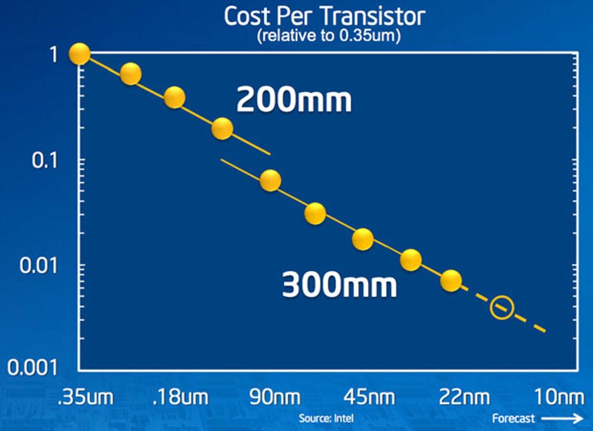
Lowering transistor costs
New manufacturing processes continue to lower the cost per transistor. This chart shows how moving from silicon wafers 200mm in diameter to 300mm wafers lowered the cost, too. The chip industry is planning a transition to 450mm wafers in coming years for a similar lowering of transistor costs.
16 of 21 Intel
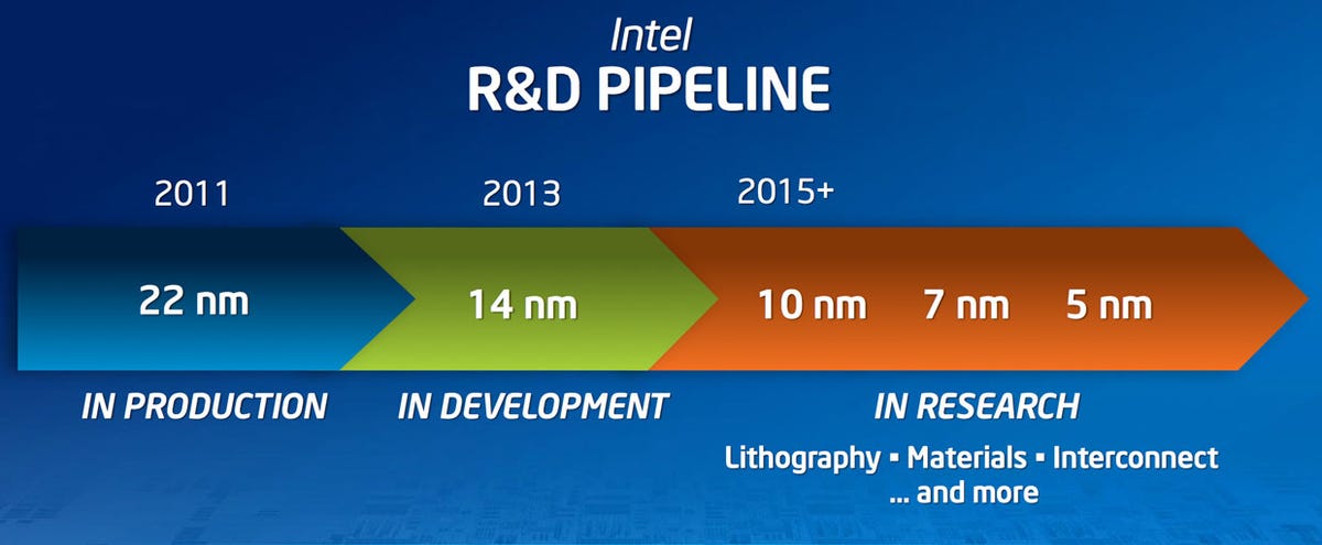
Intel's road map to 5nm chips
Intel's current chip manufacturing road map extends to the 5nm process "node," scheduled to reach chip fabs in 2019.
17 of 21 Royal Swedish Academy of Sciences
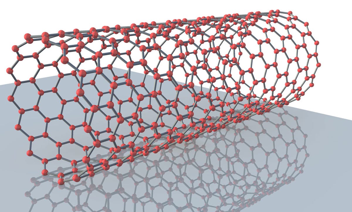
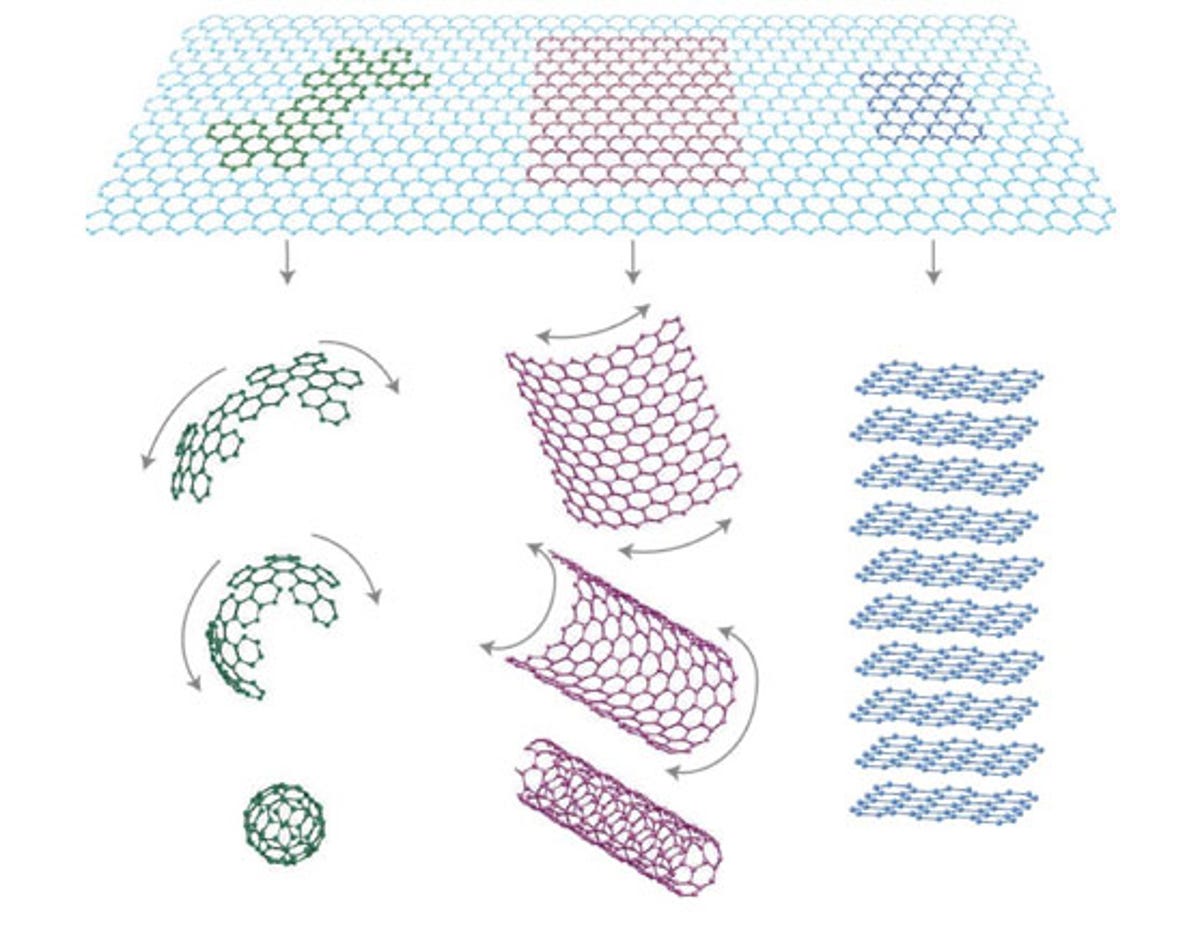
Graphite, graphene, and other carbon forms
The chickenwire-like lattice of carbon atoms just one atom thick is called graphene, one candidate for a new chip semiconductor material. Another is a cylindrical configuration called a carbon nanotube. A 60-atom sphere is called a buckyball. Many sheets of graphene makes graphite, the form of carbon used in pencil lead.
18 of 21 IBM
Dual-contact graphene transistor technology
One of the challenges in using graphene in transistors is integrating it with other parts of the chip. Here, IBM researchers show their dual-contact technique that sandwiches a graphene ribbon between two layers of electrical contact. Step a shows the bottom layer of the contact, step b shows the addition of the graphene, and step c shows the addition of the top contact.
19 of 21 IBM
IBM dual-layer graphene transistor research
This IBM illustration shows how there's less electrical noise using dual layers of graphene in semiconductor devices.
20 of 21 IBM
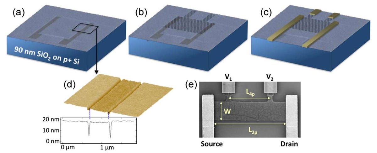
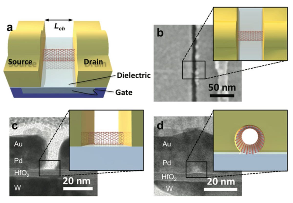
IBM carbon nanotube transistor research
IBM is working on replacing silicon channels in transistors with carbon nanotubes. These images show a schematic and real-world images of such a device. Image b shows a top view, image c shows a cross section, and image d shows an end-on view.
21 of 21 National Academy of Sciences
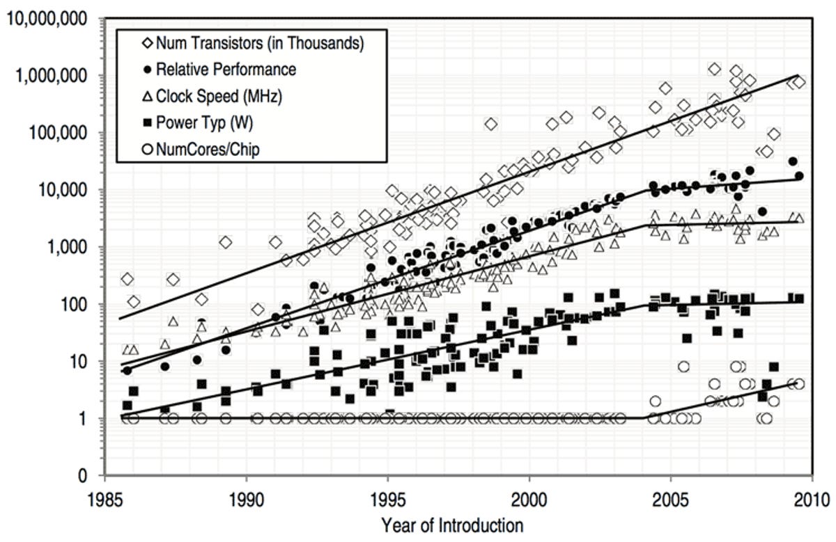
Chip power vs performance
Processor frequency increases may have stalled, but the number of transistors continues to increase, a National Academy of Sciences report showed. The transistors are used now to built multicore chips with parallel processing engines. Although relative performance isn't increasing as fast, power consumption is holding level.