Inside Samsung Semiconductor's new headquarters (pictures)
The South Korean company has built a 1.1-million-square-foot campus in San Jose, California.


A grand opening for Samsung
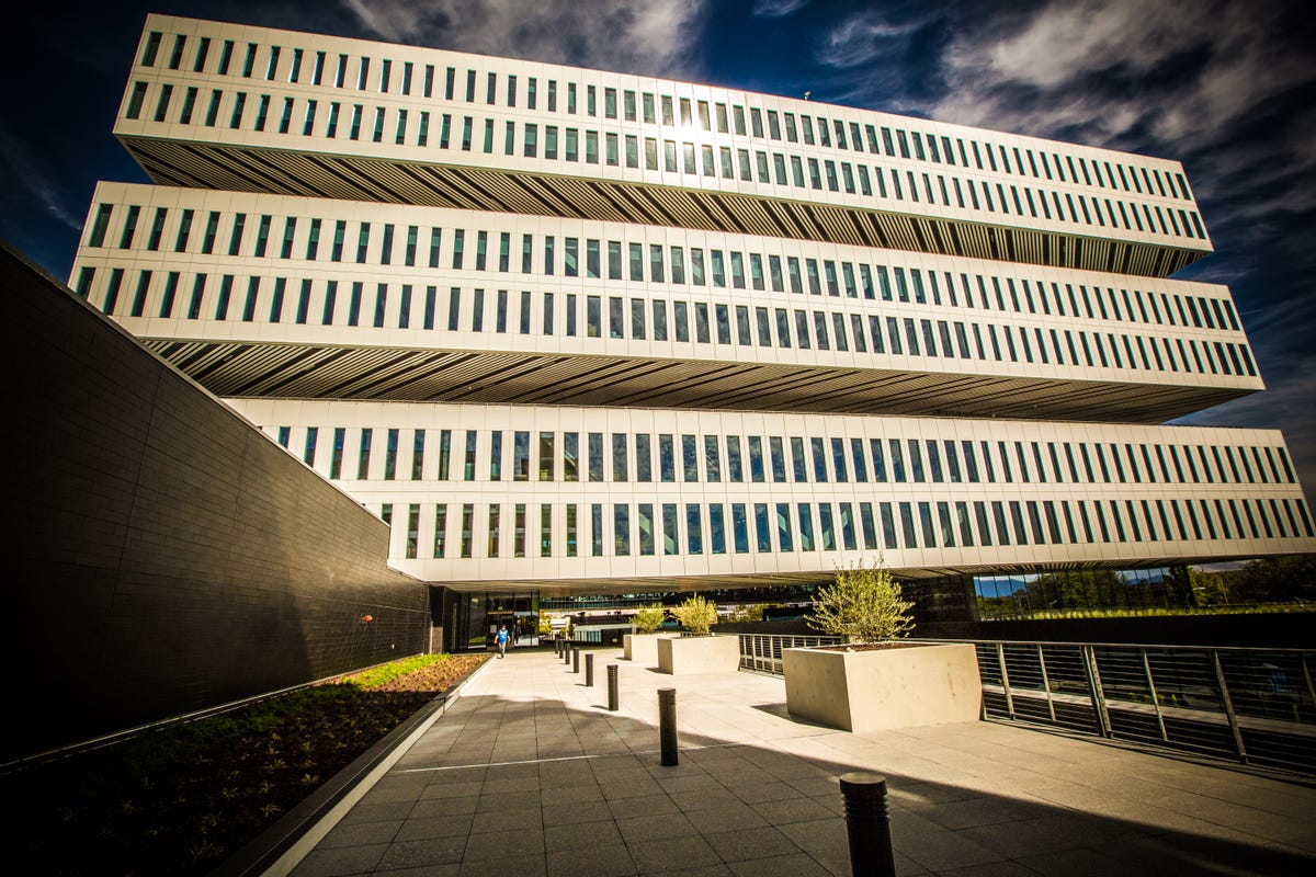
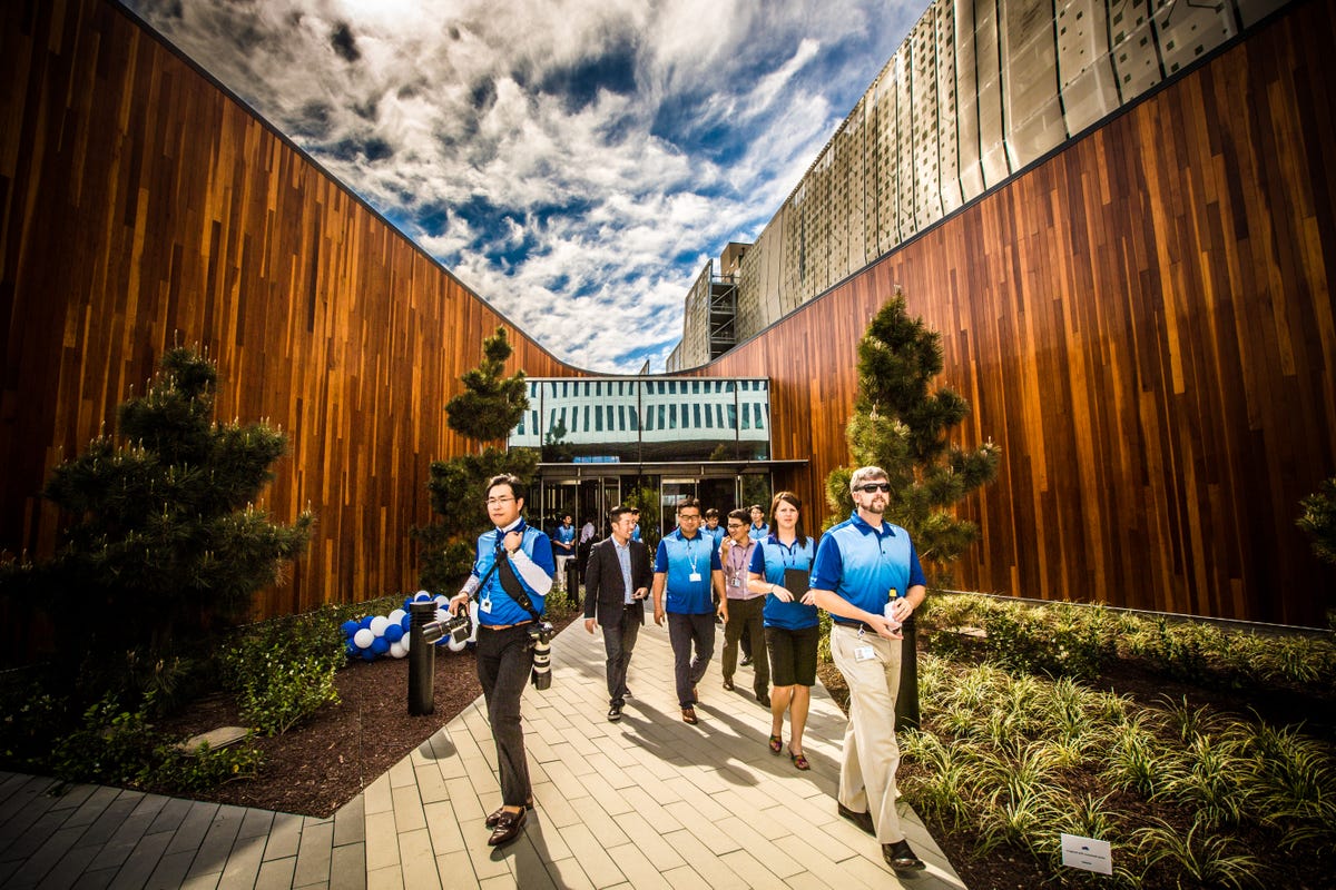
Samsung held opening ceremonies Thursday for a new 1.1 million-square-foot site that will house the Samsung Semiconductor Americas headquarters.
The $300 million campus, located north of downtown San Jose, California, houses research and development and sales operations for Samsung's US semiconductor business.
A bigger presence in Silicon Valey
"We really want to leverage the [new site] as the foundation for our presence in Silicon Valley," Jim Elliott, corporate vice president of memory marketing at Samsung, said Thursday during the company's opening ceremony.
A new space for innovation
Global architecture firm NBBJ designed site, located about 12 miles from Apple's headquarters in Cupertino, California.
The facility includes a 10-story office tower, seven-story parking garage and a green space that links the campus together.
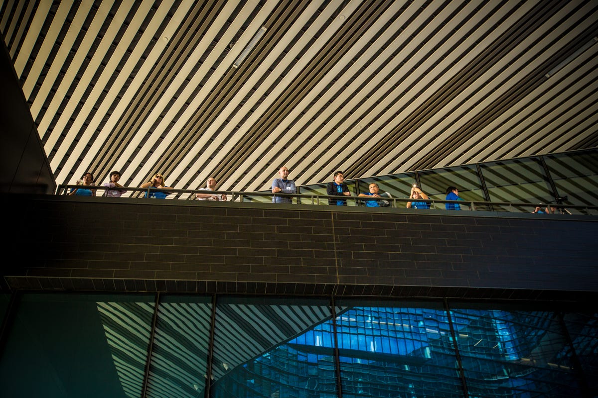
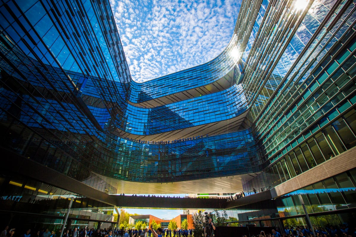
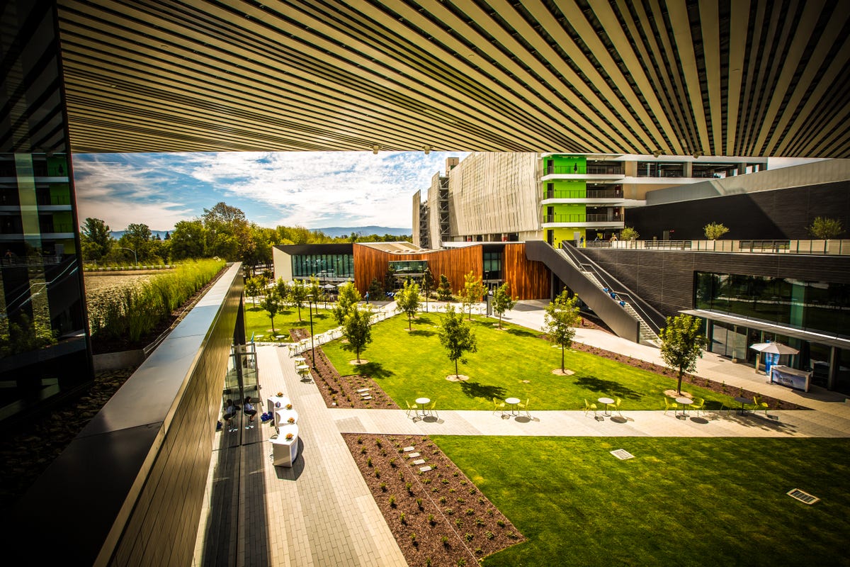
The view from above
Samsung employees overlook the center plaza of the new Samsung Semiconductor building during the opening ceremonies Thursday in San Jose, California.
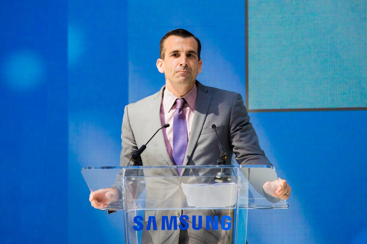
Mayor Liccardo
San Jose, California, Mayor Sam Liccardo spoke at the event.
Samsung broke ground on the building in mid-2013. The campus consolidates more than 700 Samsung employees into one location, and the company can ultimately base up to 2,000 workers there.

Dancers complete the festivities
The opening ceremony featured a music and dance troupe, Eclipse Dance Theater.
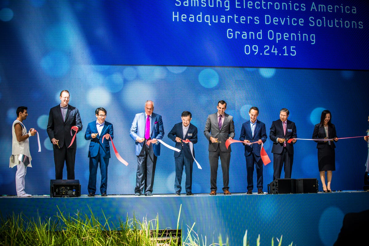
Ribbon cutting
Samsung opened the offices Thursday with a ceremony and ribbon-cutting featuring Oh-Hyun Kwon, Samsung Electronics vice chairman and co-CEO; Sam Liccardo, mayor of San Jose, California; and Chuck Reed, the former mayor of San Jose.
Open space
Samsung says the new campus' design increases collaboration by encouraging more spontaneous encounters between employees, and bringing the outdoors closer to the workplace, facilitating creativity.
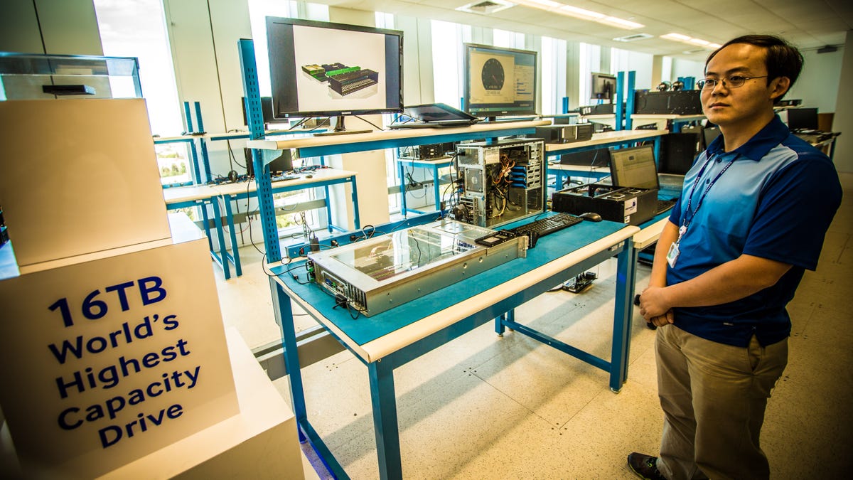
A look at operations
During a tour on Thursday, CNET had a look at the research and development operation inside the new Samsung Semiconductor building in San Jose, California.
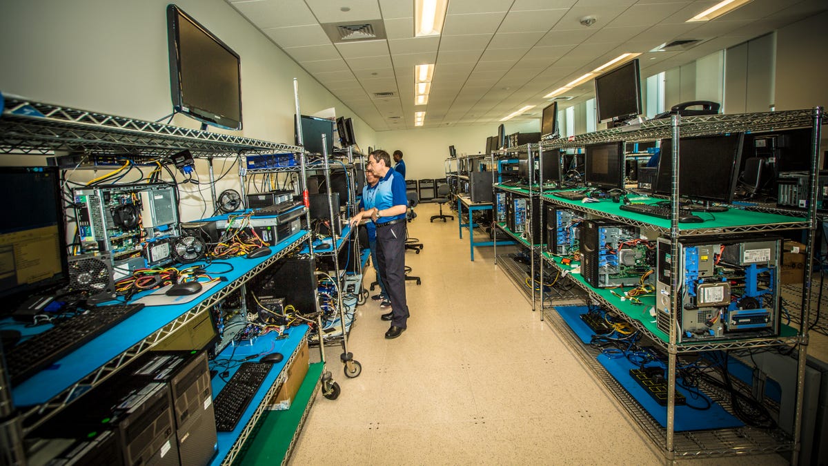
Samsung’s R&D
Samsung is the world's biggest vendor of memory chips and the second-biggest processor maker overall after Intel, and the semiconductor operations have long been at the forefront of innovation.
With the new Americas headquarters, Samsung’s R&D efforts will be substantially bolstered.
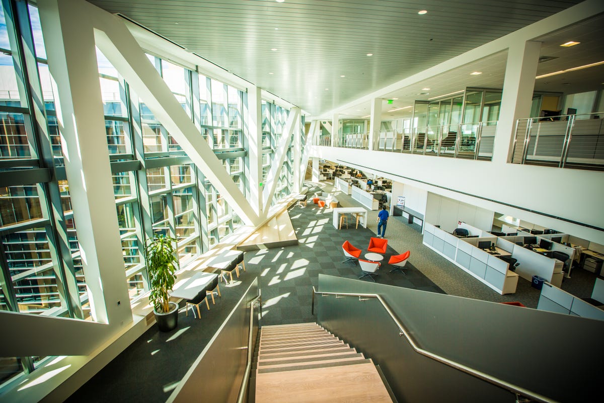
Open work spaces
A look inside at one of the open work spaces intended to facilitate collaboration and creativity.
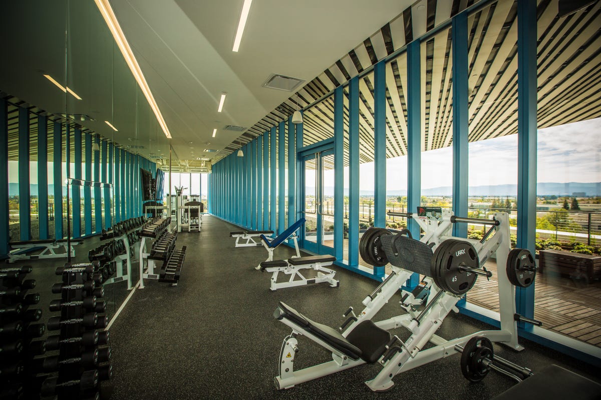
A gym with a view
A sprawling workout facility winds around the outside of the building.
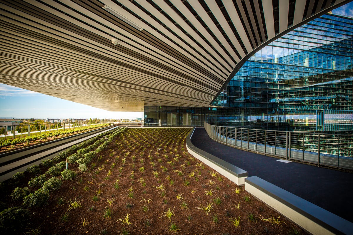
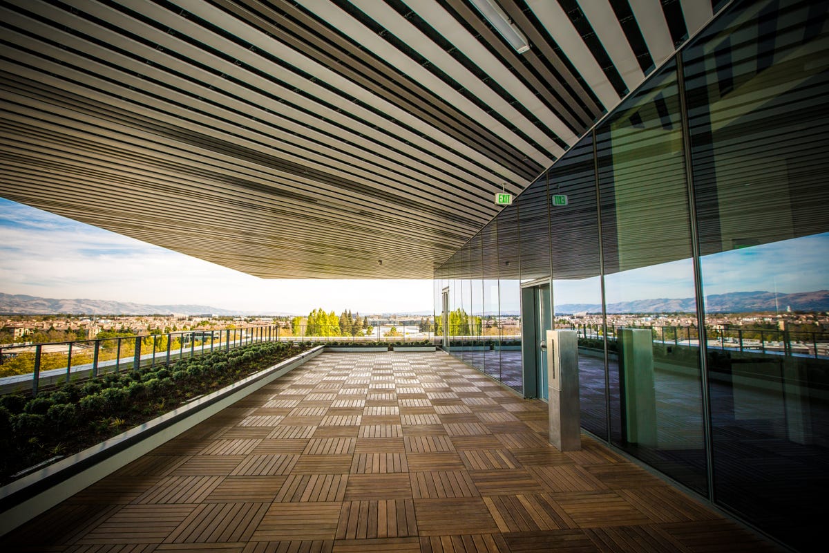
Terrace gardens
Beautiful terrace gardens take advantage of the typically beautiful, sunny climate in San Jose, California.
Tapping into local talent
Samsung has been making a bigger push into the Bay Area over the past couple of years.
Being here means Samsung can tap into local talent and have chance encounters with venture capitalists, entrepreneurs, partners and startups looking to innovate in areas where the company has struggled, such as software and services.
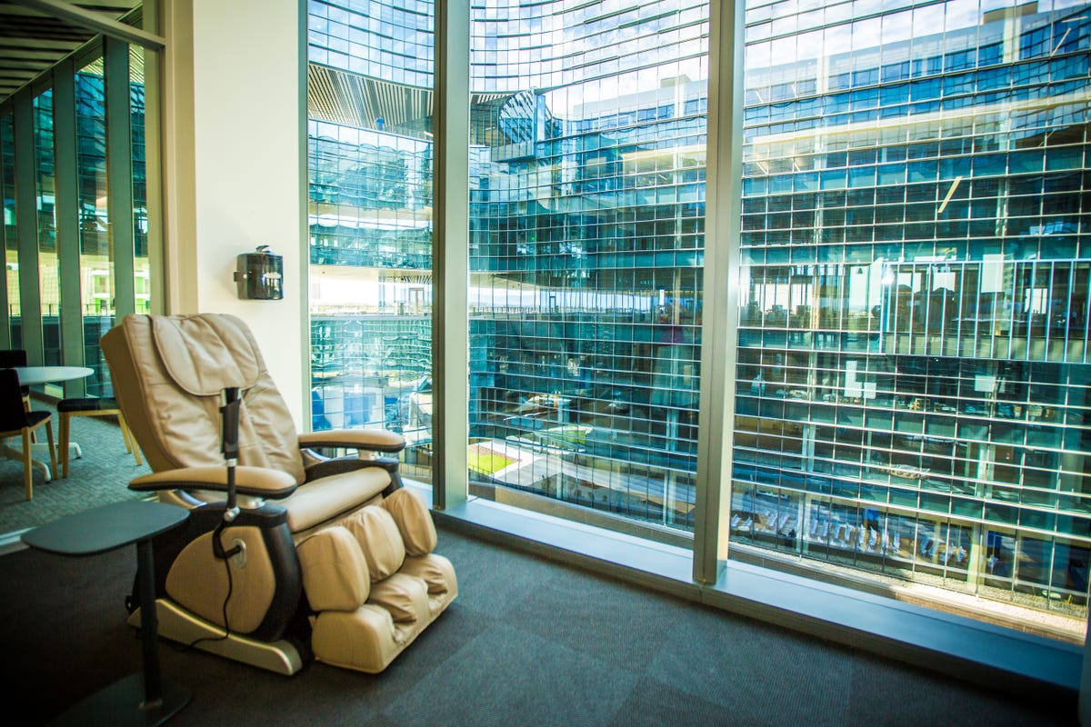
Massage chair
A massage chair looks out over the interior courtyard of the massive windowed building.
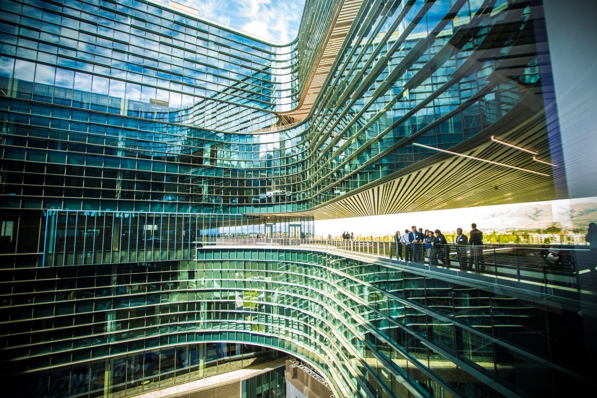
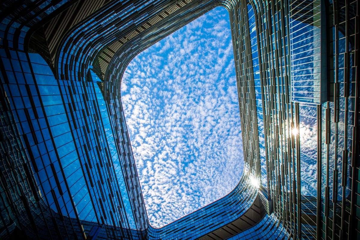
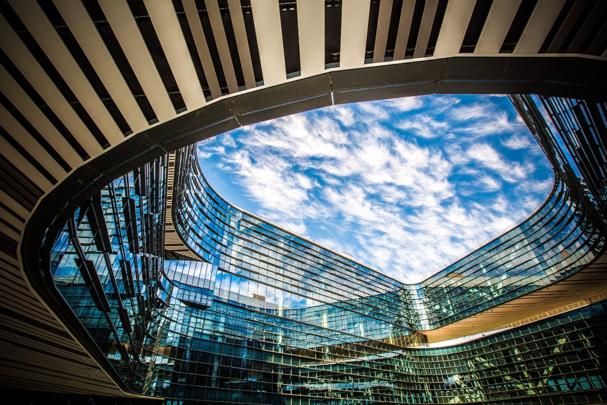
Glass curves
Open, bright and visible glass windows from floor to ceiling.
Gathering spaces
Samsung hopes the open design of the building with facilitate collaboration between employees and allow for impromptu meetings.
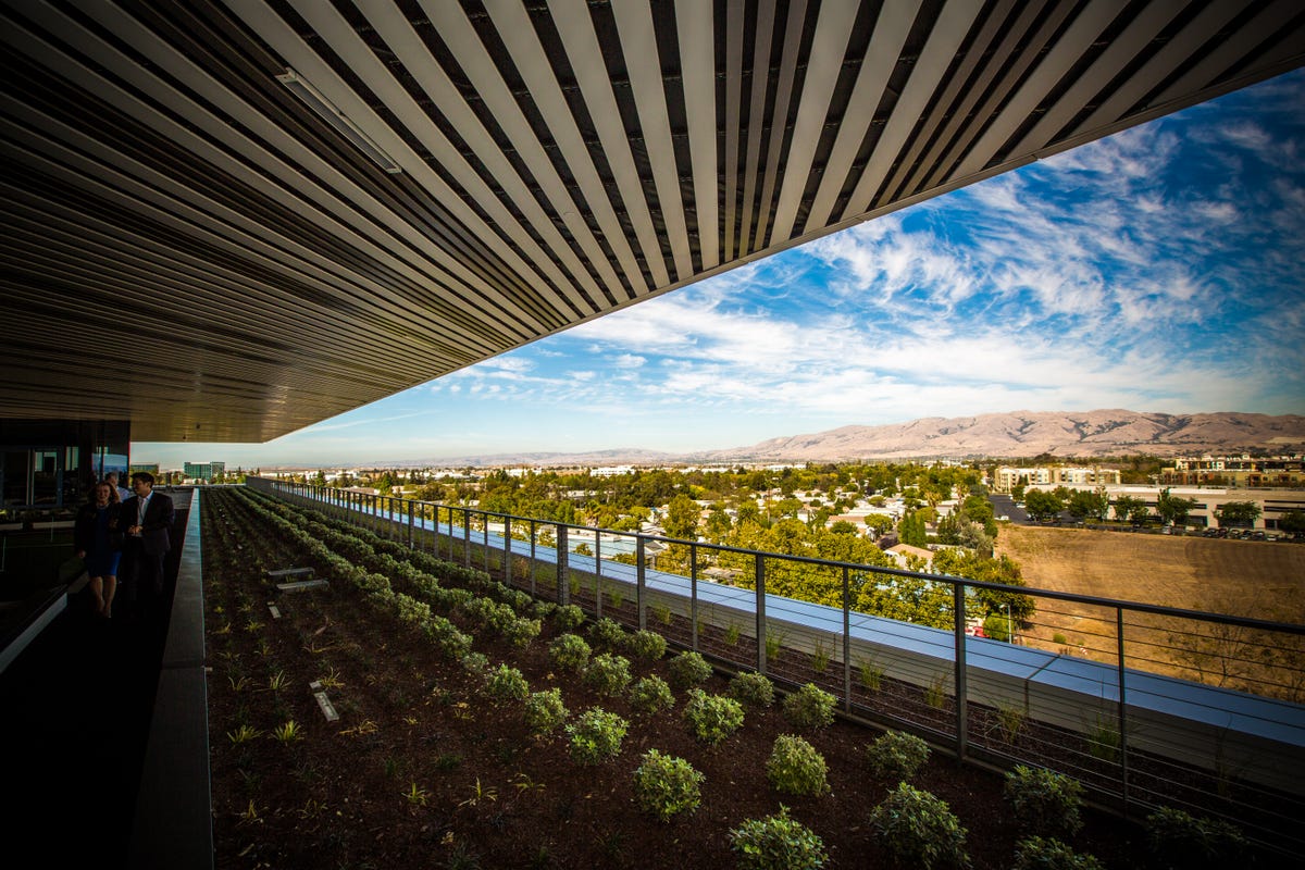
A view of San Jose
From one of the terraces, a view looking out over the hills surrounding San Jose, California.
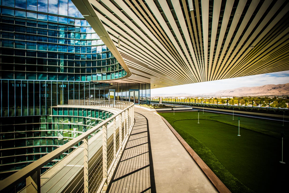
Putting green
A putting green offers a place to relax in the shade outdoors.
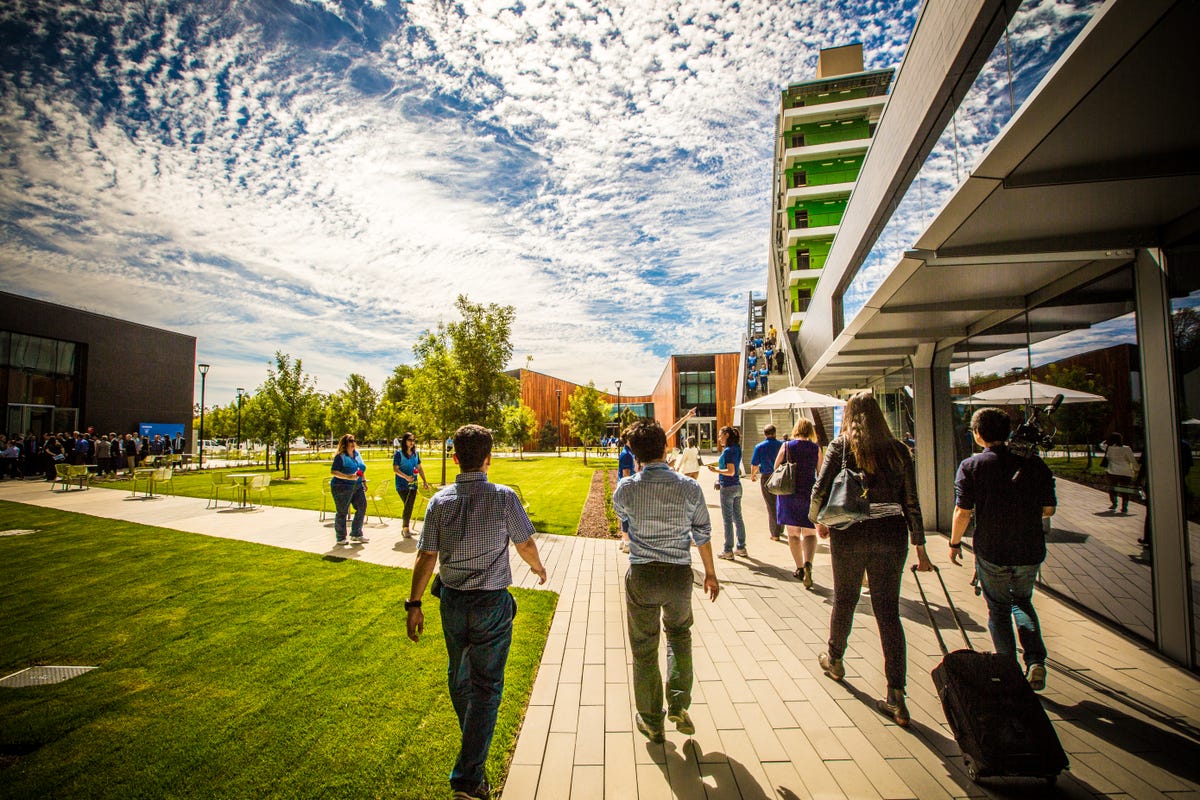
Park life
The campus grounds are green and open, with many meeting spaces, walkways, benches and other park-like features.
Break for lunch
Samsung employees exit the campus cafeteria on Thursday following the official opening of the campus.
More Galleries
My Favorite Shots From the Galaxy S24 Ultra's Camera
20 Photos
Honor's Magic V2 Foldable Is Lighter Than Samsung's Galaxy S24 Ultra
10 Photos
The Samsung Galaxy S24 and S24 Plus Looks Sweet in Aluminum
23 Photos
Samsung's Galaxy S24 Ultra Now Has a Titanium Design
23 Photos
I Took 600+ Photos With the iPhone 15 Pro and Pro Max. Look at My Favorites
34 Photos