Big Blue has developed a way to use a combination of chip patterns and chemical bonding to precisely place carbon nanotubes on computer chips. Here's a look at some of the technology involved.
Stephen Shankland
Stephen Shankland worked at CNET from 1998 to 2024 and wrote about processors, digital photography, AI, quantum computing, computer science, materials science, supercomputers, drones, browsers, 3D printing, USB, and new computing technology in general. He has a soft spot in his heart for standards groups and I/O interfaces. His first big scoop was about radioactive cat poop.
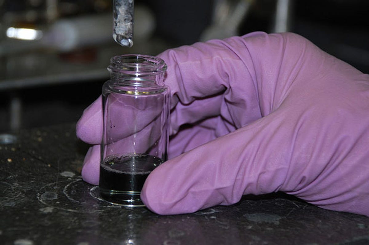
In this dark solution, IBM makes use of carbon nanutubes -- very small structures made of a lattice of carbon atoms rolled into a cylindrical shape. A team of eight researchers have figured out a way to precisely place them on a computer chip, IBM announced today. The new technique helps improve the nanotubes' chances in the hunt for alternatives once silicon transistor technology, the beating heart of today's, runs out of steam.
2 of 10 IBM
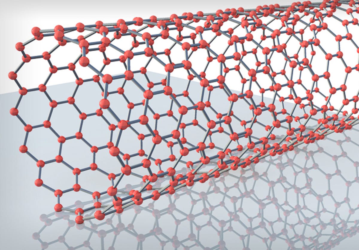
Carbon nanotube model
A model of a carbon nanotube with no end caps.
3 of 10 IBM
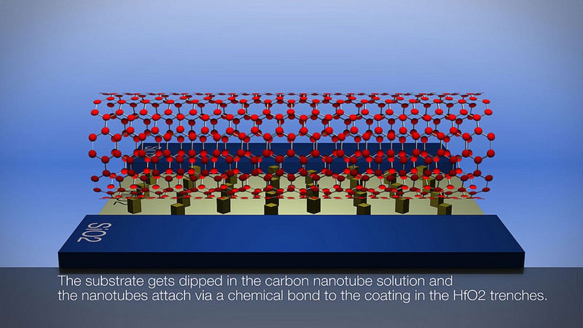
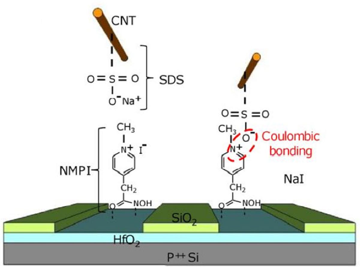
Nanotubes aligned in hafnium oxide channel
This computer model shows how carbon nanotubes bond chemically with a special coating of materials in a trench of exposed hafnium oxide.
4 of 10 IBM
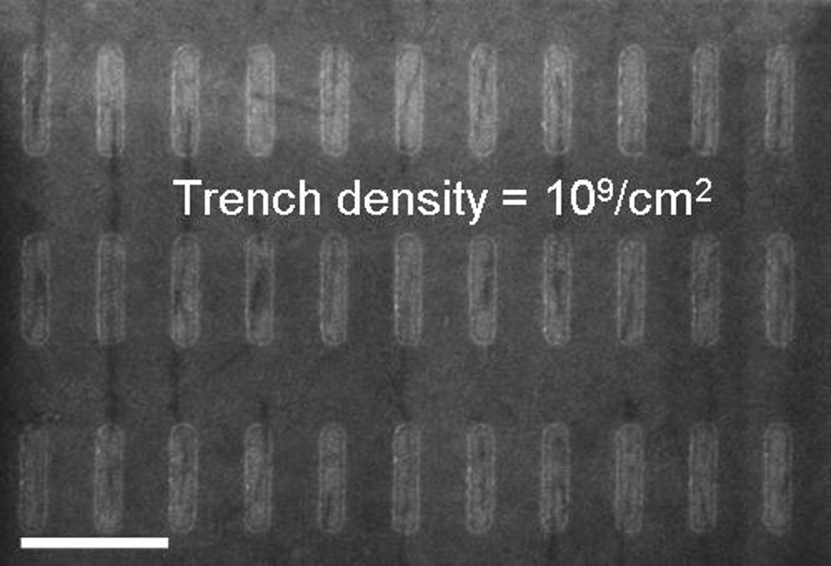
IBM carbon nanotube placement demonstration
The dark lines are carbon nanotubes that sometimes -- but not always -- are placed in trenches. The more accurately IBM can place the nanotubes, the more likely they can be used as semiconductor devices in computer chips. The density of carbon nanotubes shown here permits a billion per square centimeter.
5 of 10 IBM
IBM carbon nanotube test chip
In this close-up image, the very thin black lines are carbon nanotubes that span the gap between two electrical contacts. IBM strives to get only a single nanotube in each of the channels, visible as white outlines.
6 of 10 IBM
IBM carbon nanotube self-assembly technique
Chemical bonding attaches carbon nanotubes to channels of exposed hafnium oxide in IBM's fabrication process.
7 of 10 IBM
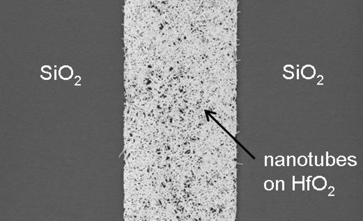
Carbon nanotubes' hafnium oxide affinity
IBM's silicon wafers have two surfaces on top, hafnium oxide and silicon dioxide. This close-up image shows speckles of carbon nanotubes that bond only with the hafnium oxide, part of IBM's approach to positioning them precisely on a chip.
8 of 10 IBM
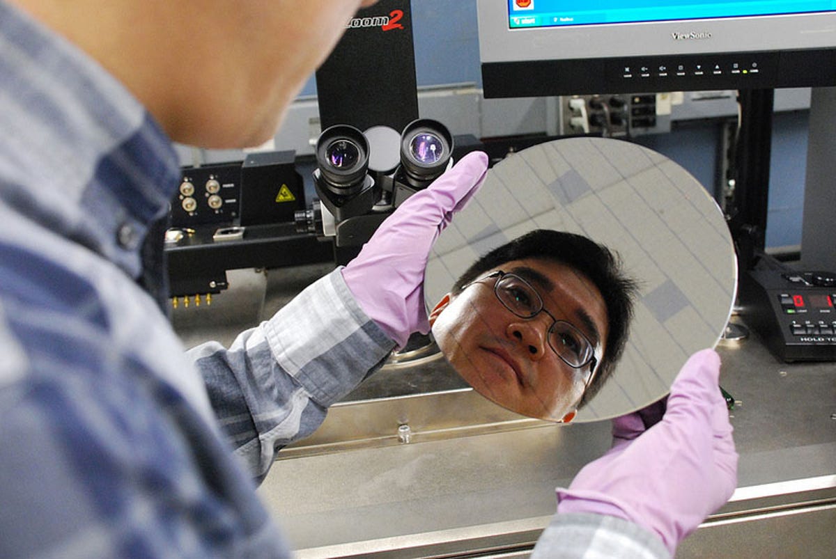
IBM Carbon nanotube chip wafer
IBM researcher Hongsik Park looks over a chip wafer with carbon nanotubes. The wafer has two surfaces, trenches made of hafnium oxide that attract carbon nanotubes in a special solution silicon oxide that doesn't.
9 of 10 IBM
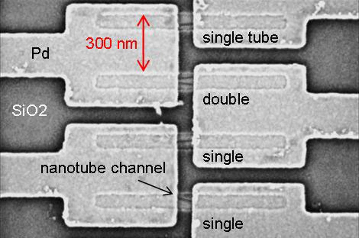
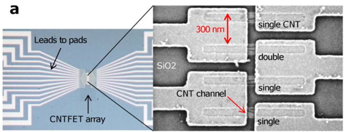
IBM carbon nanotube testing chip
IBM's technique can arrange single carbon nanotubes -- and sometimes pairs -- between two electrical contacts. It's an essential part of making a transistor in which a nanotube leads from a source on one side to a drain on the other. At left in this is an image of a chip designed to test the technology electrically; at right is a close-up of the nanotubes stretching from one electrical contact to another.
10 of 10 Royal Swedish Academy of Sciences
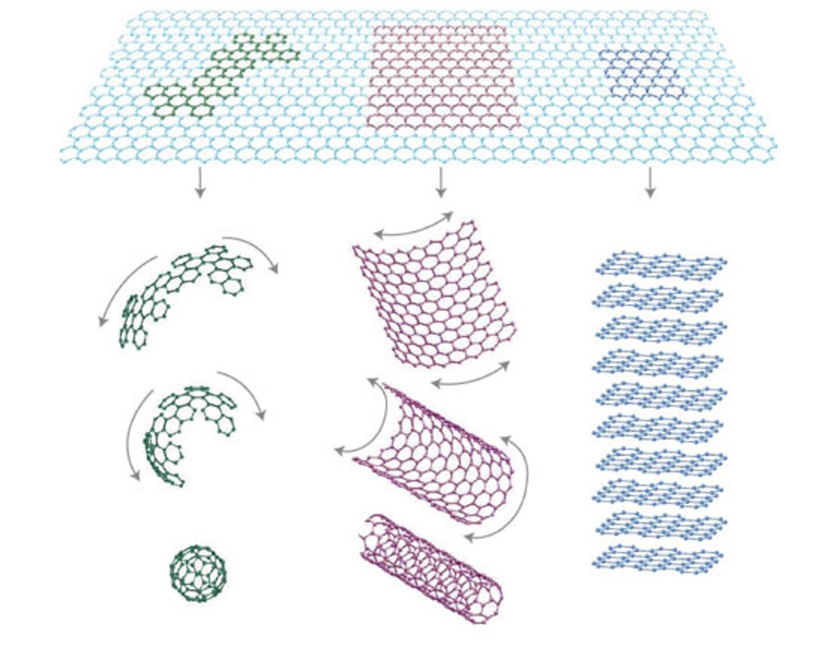
Carbon: Graphene, nanotubes, graphite
The chickenwire-like lattice of carbon atoms just one atom thick is called graphene, one candidate for a new chip semiconductor material. Another is a cylindrical configuration called a carbon nanotube. A 60-atom sphere is called a buckyball. Many sheets of graphene makes graphite, the form of carbon used in pencil lead.