A look inside Intel's mammoth Arizona chipmaking fab
Take a tour inside one of the highest-tech factories in the world, to see how Intel manufactures microprocessors.


Intel's Fab 42 in Chandler, Arizona
Fab 42 is located at Intel's newer Ocotillo campus in Chandler, Arizona. Along with Intel's older campus in the city, Intel has 12,000 employees in Chandler, but the chipmaker is hiring 3,000 more as it builds and staffs Fab 52 and Fab 62 at the same site. Here's a look inside.
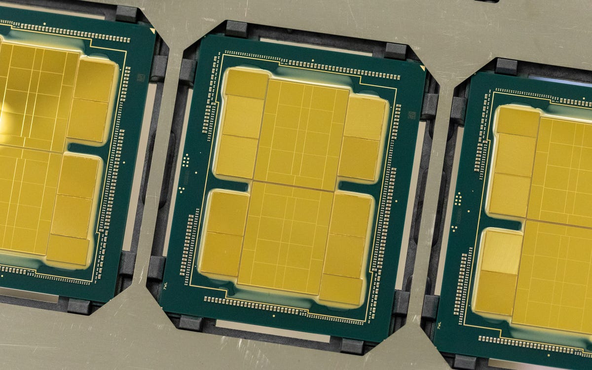
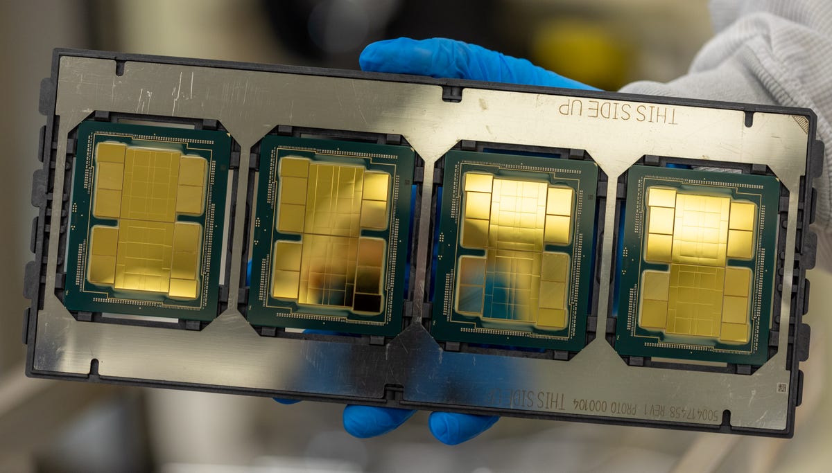
Sapphire Rapids server chip
This Sapphire Rapids server processor, due to ship in 2022 under Intel's Xeon server chip brand, comprises four larger "chiplets" housing processing engines and four smaller high-bandwidth memory modules to store data. They're all connected with Intel's high-speed EMIB links, a packaging innovation that Intel hopes will help it compete against rivals including TSMC and Samsung.
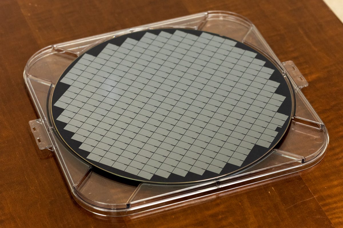
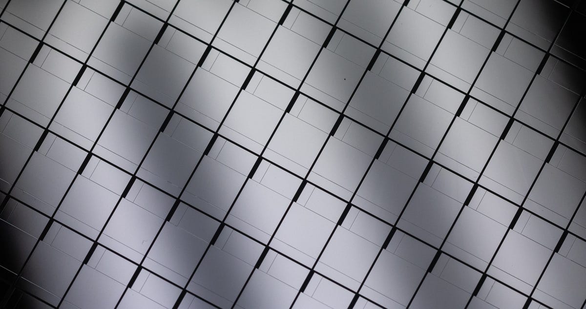
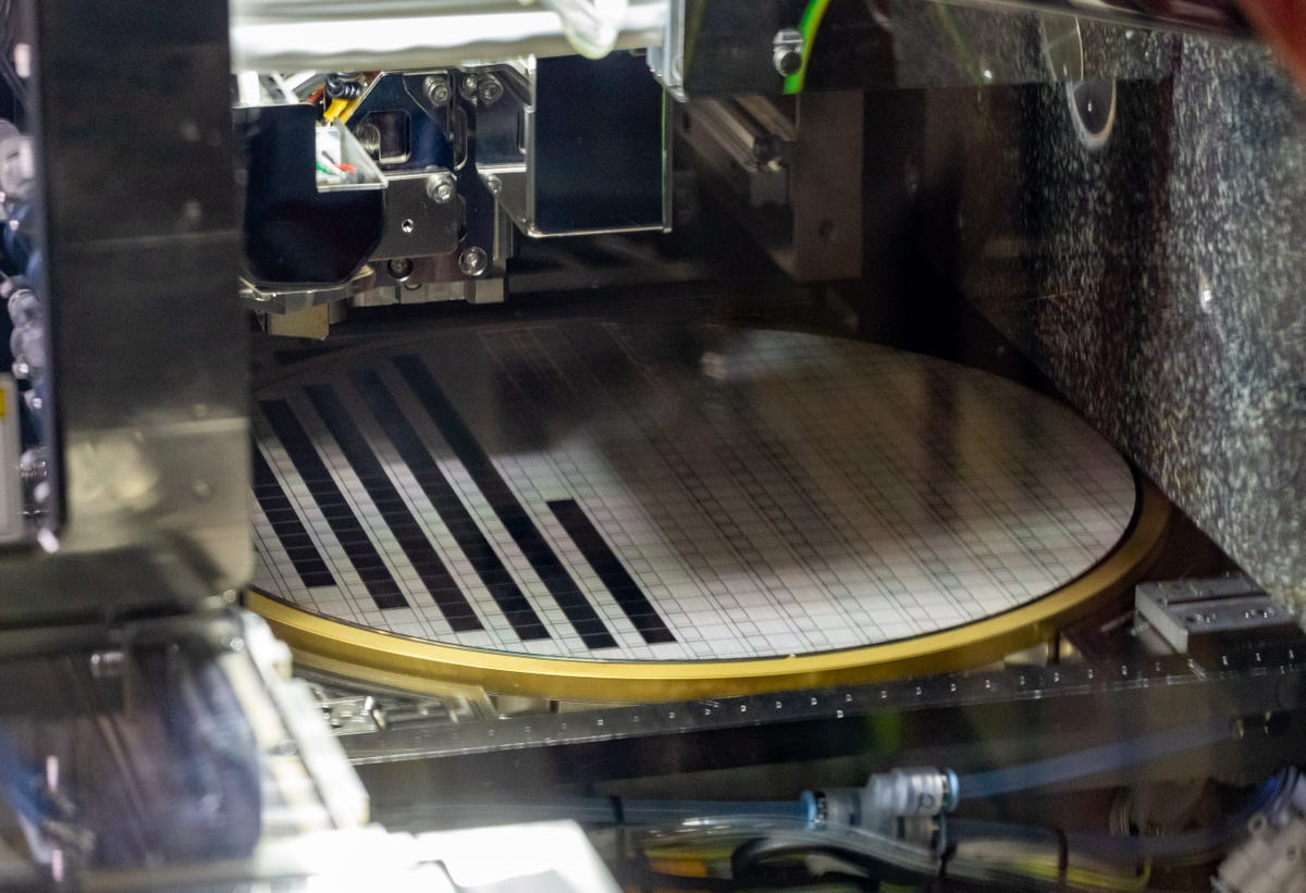
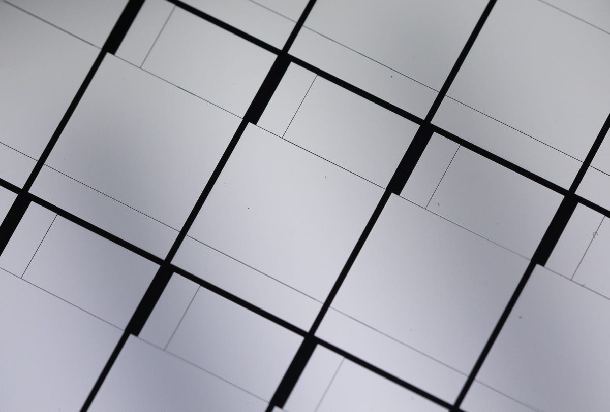
Wafer of Meteor Lake test chips
A 300mm wafer is studded with hundreds of Meteor Lake test chips. In this case, a top layer of chiplets is bonded to a base layer. Through a process called dicing, the wafer is then sliced into individual processors.
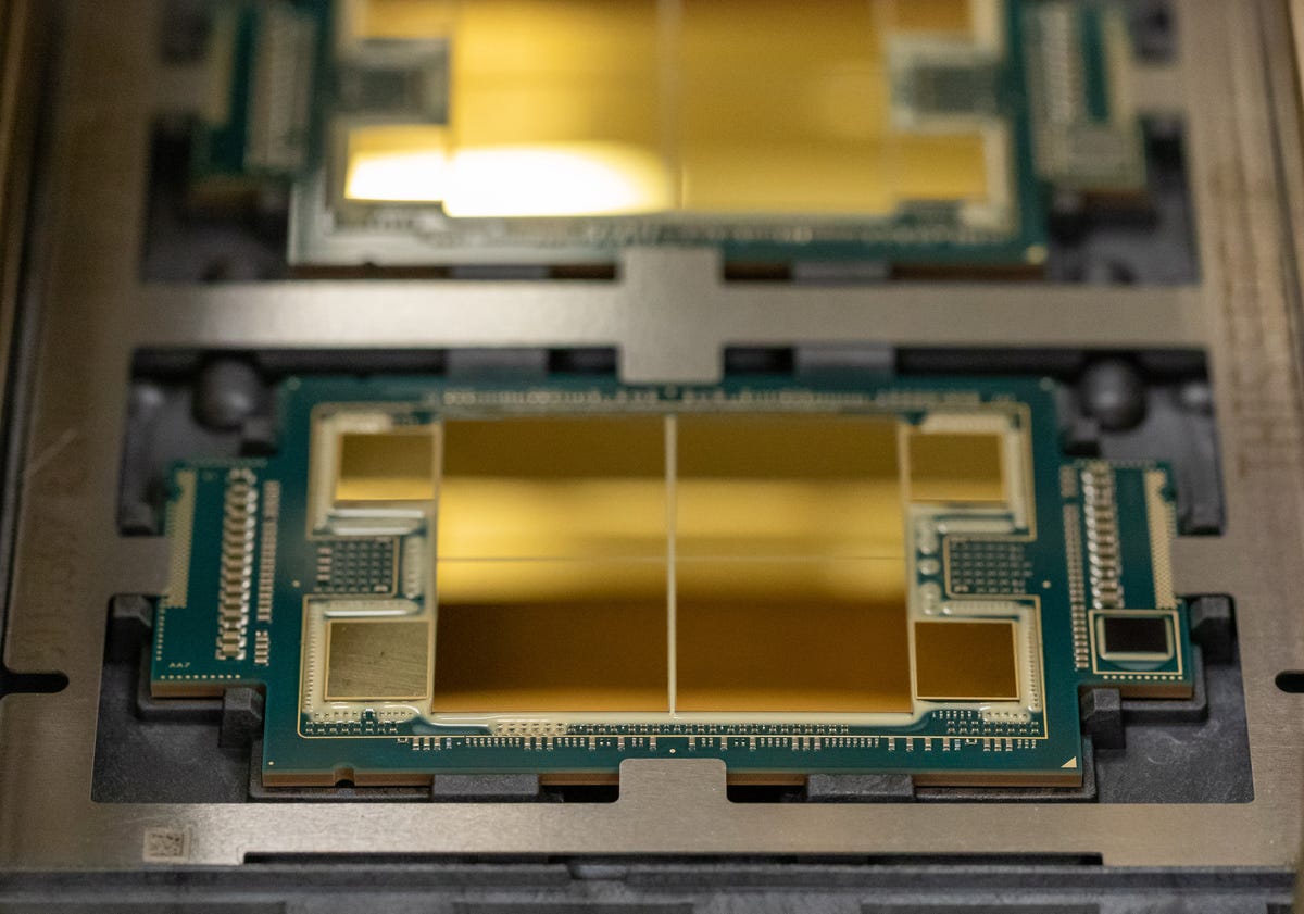
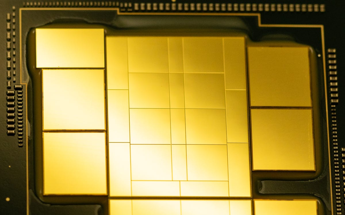
Intel Sapphire Rapids substrate
Sapphire Rapids, an Intel Xeon server chip arriving in 2022, has four processing engines and four high-bandwidth memory modules in the configuration shown here. This view shows the substrate that'll house eight of those elements, called chiplets. Narrow rectangular areas between are high-speed EMIB connections to link the chiplets. Such packaging technology is increasingly important in the chip industry.
Intel Ponte Vecchio processor
Intel's Ponte Vecchio processor, due to ship in 2022, is the brains of the Energy Department's Aurora supercomputer. An Intel delay held up the machine's arrival at Argonne National Laboratory, but Intel says its peak performance is double what was planned.
Chiplets on Intel Ponte Vecchio processor
Intel's Ponte Vecchio processor is a technological tour de force that combines 47 separate active silicon elements. Each chiplet is carefully bonded in a stack that sprawls outward using Intel EMIB connections and upward with Intel Foveros, an example of Intel's packaging prowess. Intel relies on its rival TSMC to build the graphics processing units at the heart of the processor.
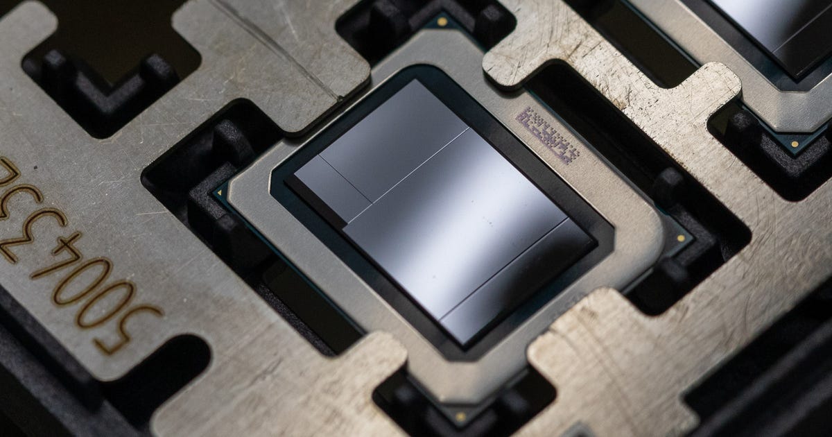
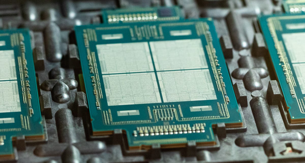
Meteor Lake test chips
Meteor Lake, a PC chip due to ship in 2023, uses a second generation of Intel's Foveros technology to stack chiplets into a full processor. This Meteor Lake test vehicle is used to ensure the Foveros packaging is working correctly, with no alignment or electrical connection problems.
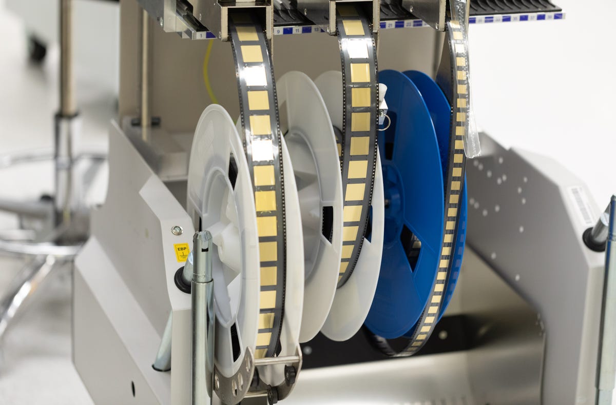
Intel Sapphire Rapids chiplets
Spools of plastic-sheathed "chiplets" flown from an Intel fab in Oregon are fed into chipmaking equipment in Intel's CH-4 fab that carefully places each silicon slice to make a larger processor.
Meteor Lake test chips
Meteor Lake test chips are squeezed side by side on a 300mm Intel wafer, with some processing elements individually bonded to others on the wafer's base layer below. This PC chip is due to ship in 2023. These are test chips to validate Intel packaging technology, not fully functioning processors.
Meteor Lake packaging tests
Meteor Lake, powering PCs arriving in 2023, combines multiple chiplets into one larger processor using Intel's Foveros packaging technology. That stacks chiplets vertically and links them with high-speed data connections. Here, individual chiplets are bonded to a bottom base wafer layer made of uncut chips.
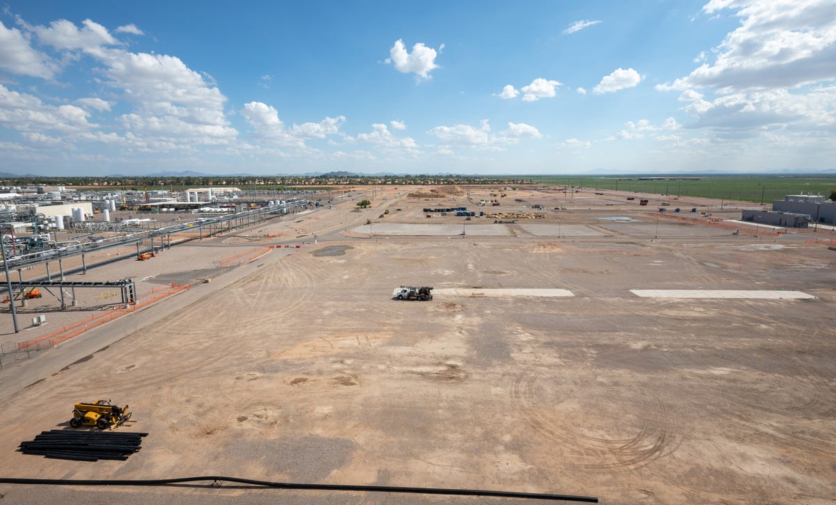
Site of Intel Fab 52 and Fab 62
This empty dirt lot in Chandler, Arizona, is where Intel has begun building Fab 52 and Fab 62, a pair of chip factories costing $10 billion each that should go online in 2024. The new fabs should add about 3,000 jobs on top of today's 12,000 for Intel's Arizona operations.

Intel street signs at Fab 42
Intel street signs at Fab 42, at its Octotillo campus near Phoenix, have chipmaking-related names like Wafer Way, Angstrom Avenue, Cleanroom Corner, Transistor Terrace, Processor Parkway, Silicon Street, and Tick-Tock Trail.
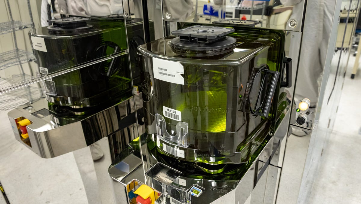
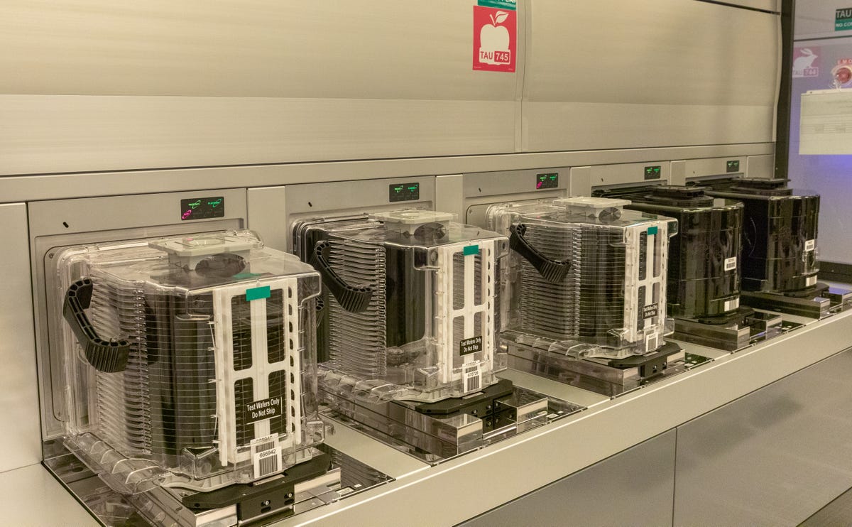
Intel chip FOUP
Fabs are extraordinarily clean facilities, but chips are protected further within FOUPs -- front opening unified pods -- that are used to shuttle stacks of silicon wafers from one manufacturing step to another. Here, two FOUPs are mounted to the front of a chipmaking equipment module.
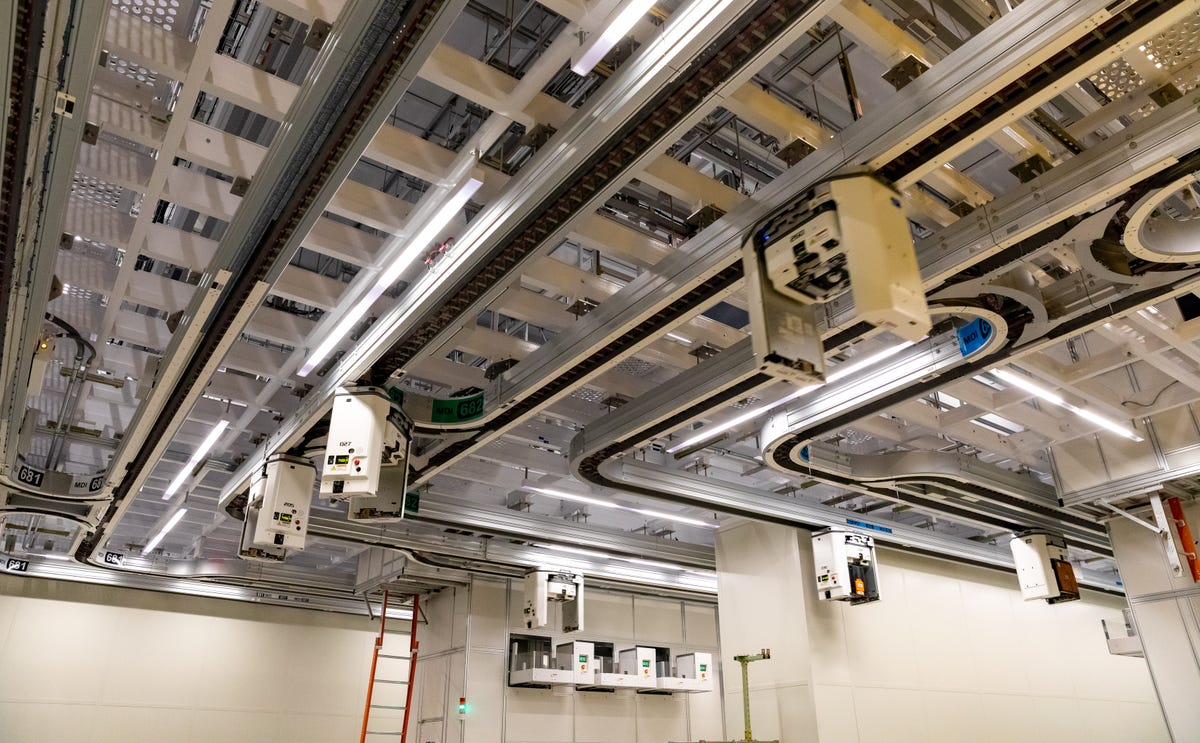
Ceiling-mounted chip transport at Intel's Fab 42
Chipmaking equipment at Intel's fab 12, 22, 32 and 42 is connected with miles of ceiling tracks that shuttle plastic pods with stacks of silicon wafers.
Intel's enormous Ponte Vecchio processor
Intel's Ponte Vecchio processors -- four are shown here side by side -- are enormous by chipmaking standards. Each has dozens of interlinked chiplets with a total of more than 1 billion transistors, the fundamental data-processing element on a chip.
Meteor Lake test chips
Individual chiplets are visible in this closeup of Meteor Lake test chips.
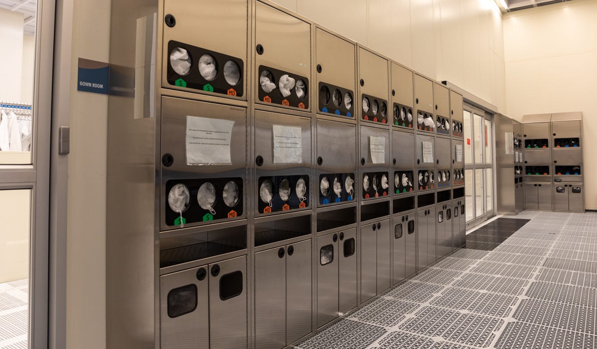
Cleanroom suit stage one: Gloves
The first step in entering a fab's cleanroom is donning two sets of gloves from a wall dispenser. The outer pair is worn only long enough to put the full protective suit on.

Intel's Fab 42 in Chandler, Arizona
Intel's Fab 42 is an enormous presence in Chandler, Arizona. It's linked to the earlier fabs 12, 22 and 32, and Intel has begun construction on the neighboring fabs 52 and 62 that'll go online in 2024.
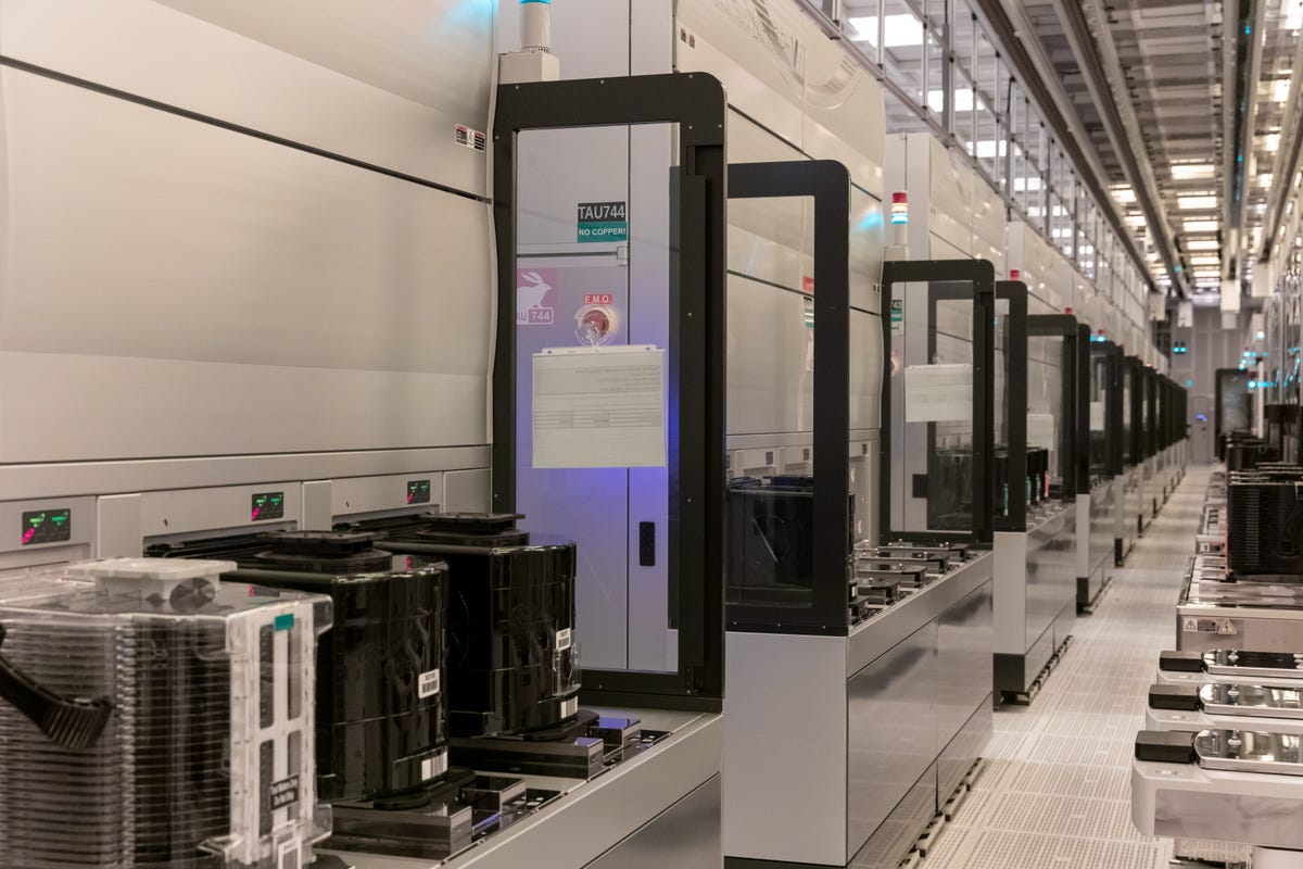
FOUPs in Intel Fab 42
Plastic pods called FOUPs carry stacks of silicon wafers from one chip manufacturing step to another. It takes hundreds of steps to make a finished processor.
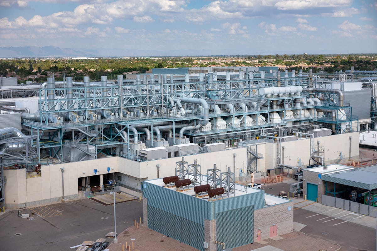
Fab 42 infrastructure
Fabs come with sprawling structures of support equipment to handle things like supplying power, purifying water and cooling air. It takes millions of gallons of pure water to run a fab. The Ocotillo campus can treat more than 9 million gallons of water every day, and Intel is working on improvements so that by 2030 it returns more water to parched southern Arizona watersheds than it uses.
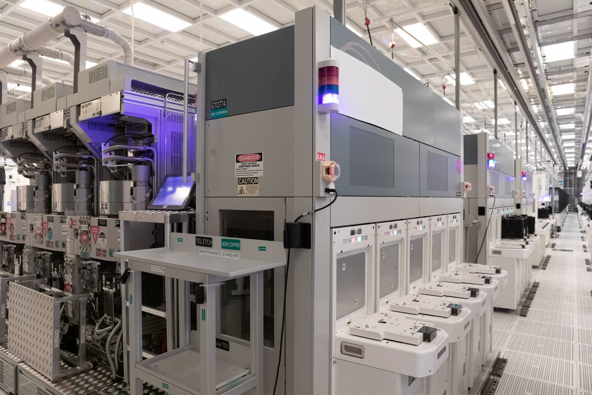
Intel Fab 42 etching equipment
One step in the chipmaking process at Intel's Fab 42 is etching equipment that removes layers of material from the surface of the silicon wafer.
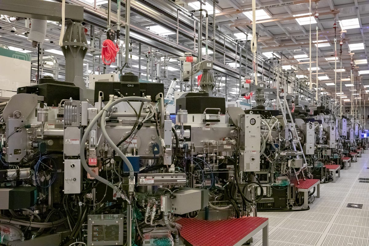
Chemical vapor deposition equipment
Chipmaking requires many steps of applying materials to a silicon wafer, zapping them with a patterned light to alter the wafer surface, then treating that surface to add and remove material. Vapor deposition is one of the methods used to add layers to the wafer.
Intel Fab 42 cleaning equipment
Chemical cleaning is one necessary step that must be repeated often while processing wafers into chips. Here plastic pods filled with silicon wafers link up to a bank of such machines.
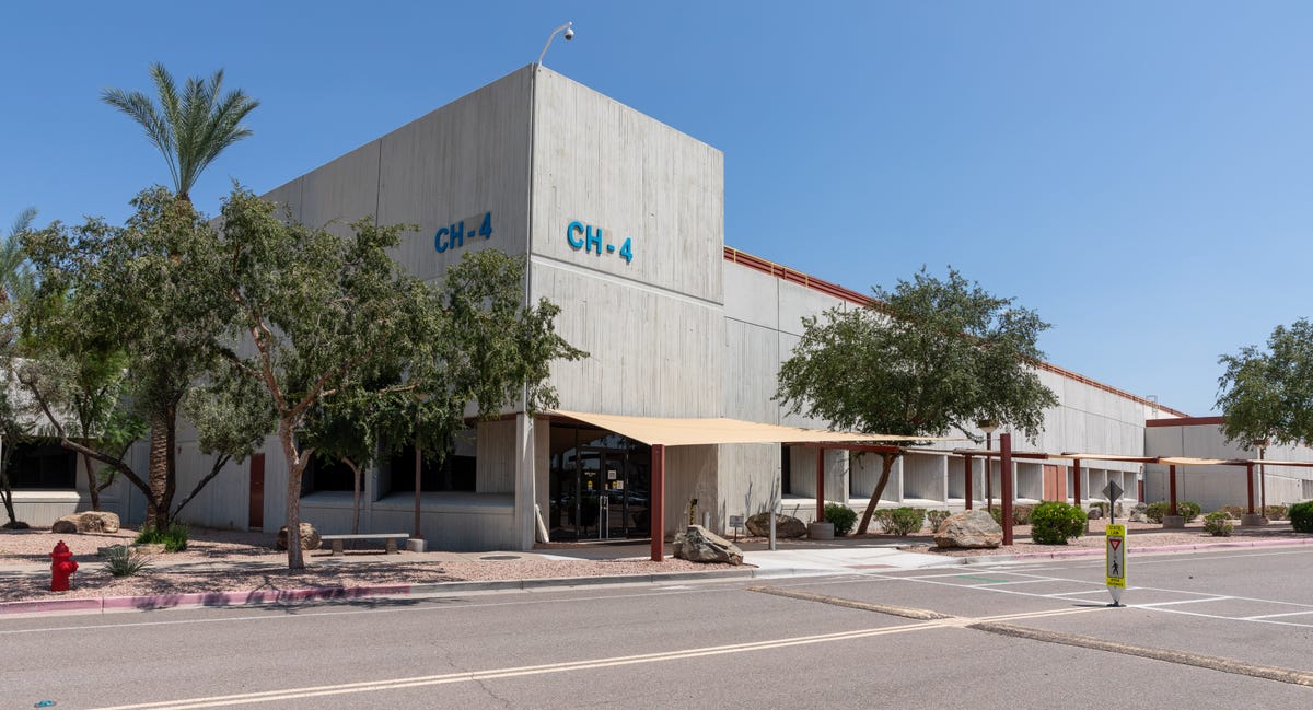
Intel CH-4 fab for chip packaging
Intel's CH-4 fab, originally built in 1980 to manufacture 80286 chips, now houses Intel's advanced packaging work to link multiple chiplets into one larger processor. That's a key part of Intel's effort to catch up to its chipmaking rivals in coming years.
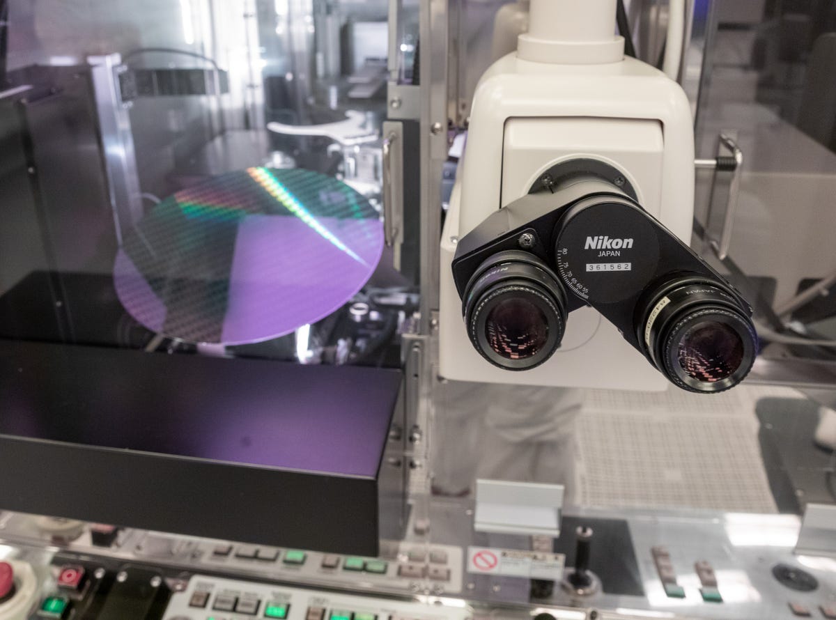
Intel fab inspection station
Silicon wafers are constantly measured and tested through the hundreds of steps it takes over about three months to turn them into silicon chips. Most of that inspection is automated, but this station lets humans take a close look, too. The wafer is the purple and green wafer to the left of the eyepieces.
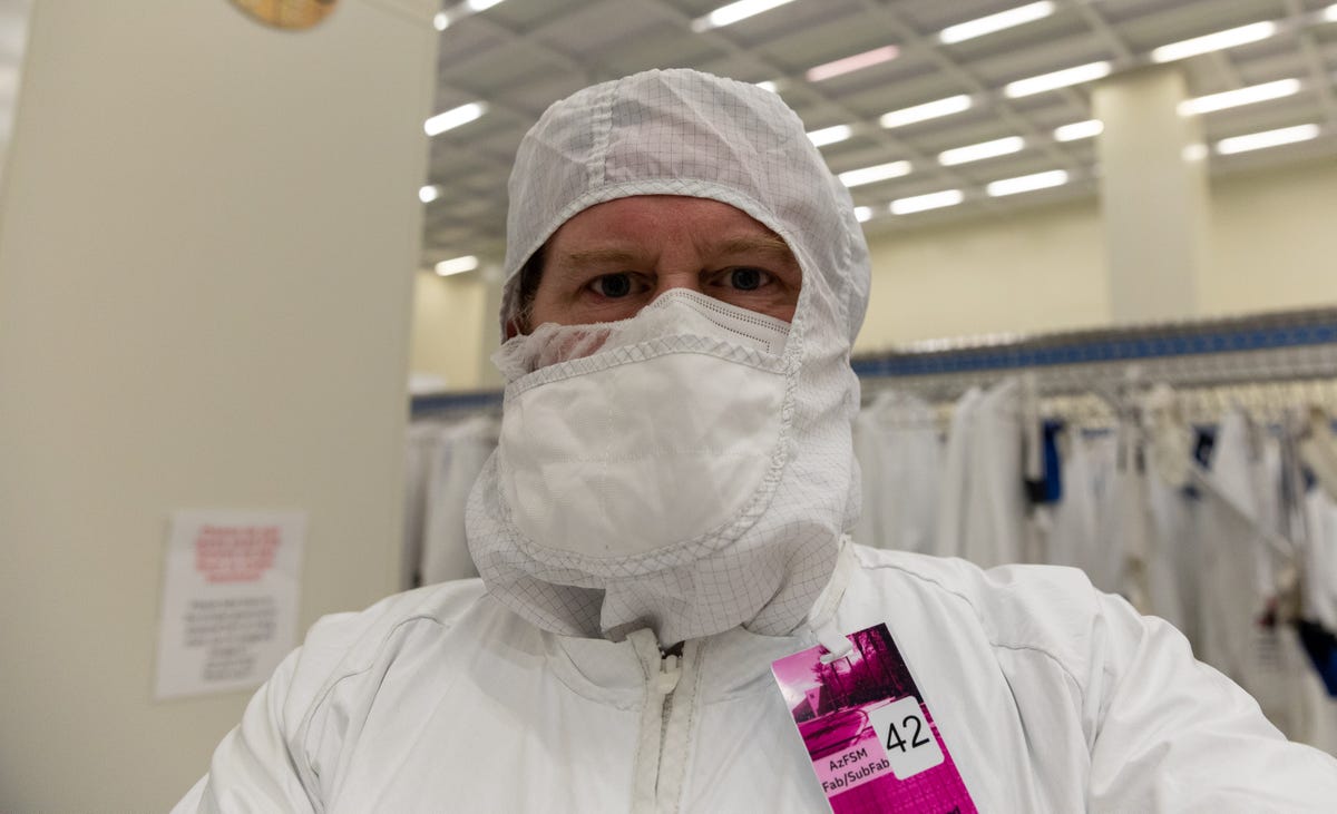
Visiting at Fab 42
CNET reporter Stephen Shankland at Intel's Fab 42 in Arizona.
More Galleries

My Favorite Shots From the Galaxy S24 Ultra's Camera
20 Photos
Honor's Magic V2 Foldable Is Lighter Than Samsung's Galaxy S24 Ultra
10 Photos
The Samsung Galaxy S24 and S24 Plus Looks Sweet in Aluminum
23 Photos
Samsung's Galaxy S24 Ultra Now Has a Titanium Design
23 Photos
I Took 600+ Photos With the iPhone 15 Pro and Pro Max. Look at My Favorites
34 Photos