Wonder material graphene taught to act electronically
Rice University researchers develop a technique to modify the surface of graphene, a step toward controlling it like a semiconductor for multi-purpose electronic circuits, optics, and chemical sensors.


Rice University researchers are bending graphene to meet their needs with a technique that promises progress on the road to nano-scale electronic circuits.
In a paper published yesterday in Nature Communications, researchers describe a way to alter graphene into "hybrid superlattices," a material potentially suitable for electronics and optical devices.
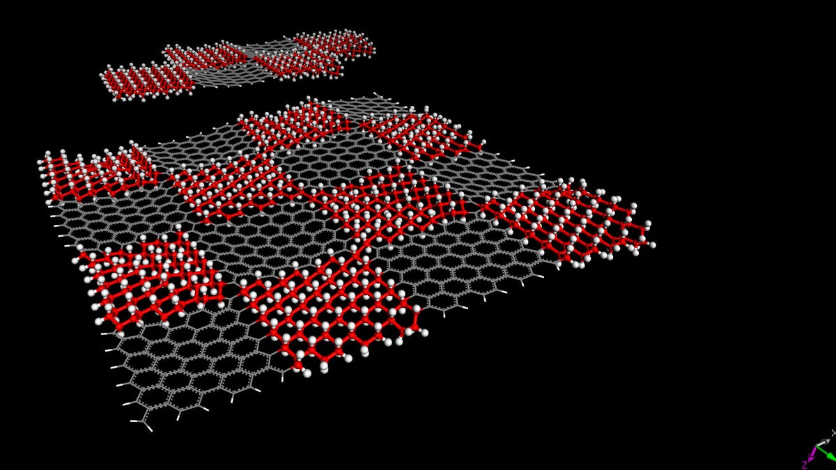
Graphene, which is a one-atom thick layer of carbon atoms interconnected in a honeycomb structure, is touted as a wonder material for a variety of uses, including faster and smaller electronics. As a material, it has excellent electrical conductivity but because it is a semimetal, researchers are still seeking ways to stop the flow of electrons, which would make it usable as a semiconductor.
Rice researchers in James Tour's labs have developed a technique to alter the surface of graphene by attaching hydrogen atoms. Making that hydrogenate graphene material, which is called graphane, paves the way for engineers to control graphene as a semiconductor for specific purposes, such as electronics and optics.
Over time, researchers hope to precisely manipulate the chemistry of graphene lattices so that special-purpose nano-scale circuits can be designed onto a surface.
"We want to make functional changes to materials where we can control the position, the bond types, the functional groups and the concentrations," said project lead Zhengzong Sun in a statement. "In the future--and it might be years--you should be able to make a device with one kind of functional growth in one area and another functional growth in another area. They will work differently but still be part of one compact, cheap device."
Controlling the molecular structure attached to graphene also has applications in chemical sensors, according to Rice. Specifically patterned materials could lead to graphene-based devices for recognizing specific organic molecules.