Sony to dump $996 million into CMOS imaging production
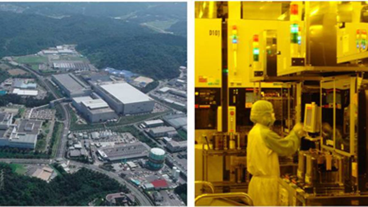
Company says the investment will be handed over to its Semiconductor's Nagasaki Technology Center over a one-year period.


Sony sees an opportunity in CMOS image sensors and is investing serious cash into them to prove it.
The company today announced that it plans to invest about 80 billion yen ($996 million) into the Sony Semiconductor Corp.'s Nagasaki Technology Center. The funds will start flowing in the first half of the fiscal year that ends March 31, 2013 and will be cut off in the first half of its next fiscal year.
Sony's investment is designed to increase total production capacity for CCD and CMOS image sensors to approximately 60,000 wafers per month by the end of September 2013. The company didn't say how many wafers are produced at this point.
Sony's Semiconductor Corp. supplies components to a host of vendors for their digital cameras and smartphones. Sony said it plans to boost its semiconductor business by including stacked CMOS image sensors in a host of other products, including those in its digital imaging and mobile businesses. Regardless of its implementation, Sony's stacked CMOS image censors are designed to be as compact as possible, enabling vendors to build smaller digital cameras and mobile devices.
Sony's investment is part of its broader "One Sony" initiative, designed to refocus its business on "three core pillars" -- digital imaging, gaming, and the mobile market. That initiative kicked off earlier this year with the promotion of Kazuo Hirai into Sony's CEO spot.