On the Moore's Law hot seat: Intel's Mike Mayberry (Q&A)
This Intel vice president lives 10 years in the chip technology future, charting a course for the computing industry and transforming research ideas into high-volume manufacturing.


- Shankland covered the tech industry for more than 25 years and was a science writer for five years before that. He has deep expertise in microprocessors, digital photography, computer hardware and software, internet standards, web technology, and more.
Mike Mayberry, perhaps more than anyone, is the guy who keeps Moore's Law ticking.
As the vice president who leads Intel's research team, he bears responsibility for making sure his employer can cram ever more electronic circuitry onto computer chips. Intel co-founder Gordon Moore 47 years ago observed the pace at which microchips' transistor count doubled, and Mayberry is in charge of keeping that legacy intact.
A lot rests on Moore's Law, which in a 1975 update to Moore's original 1965 paper predicted that the number of transistors will double every two years. That means a chip of a given size has been able to accomplish more and more computing chores -- or that you can perform the same computing tasks using a smaller, cheaper, less power-hungry chip.

Thanks to Moore's Law, the power of a supercomputer trickled down to personal computers and now to smartphones. It's proved remarkably long-lived, despite any number of crises that threatened to stall the steady march of progress.
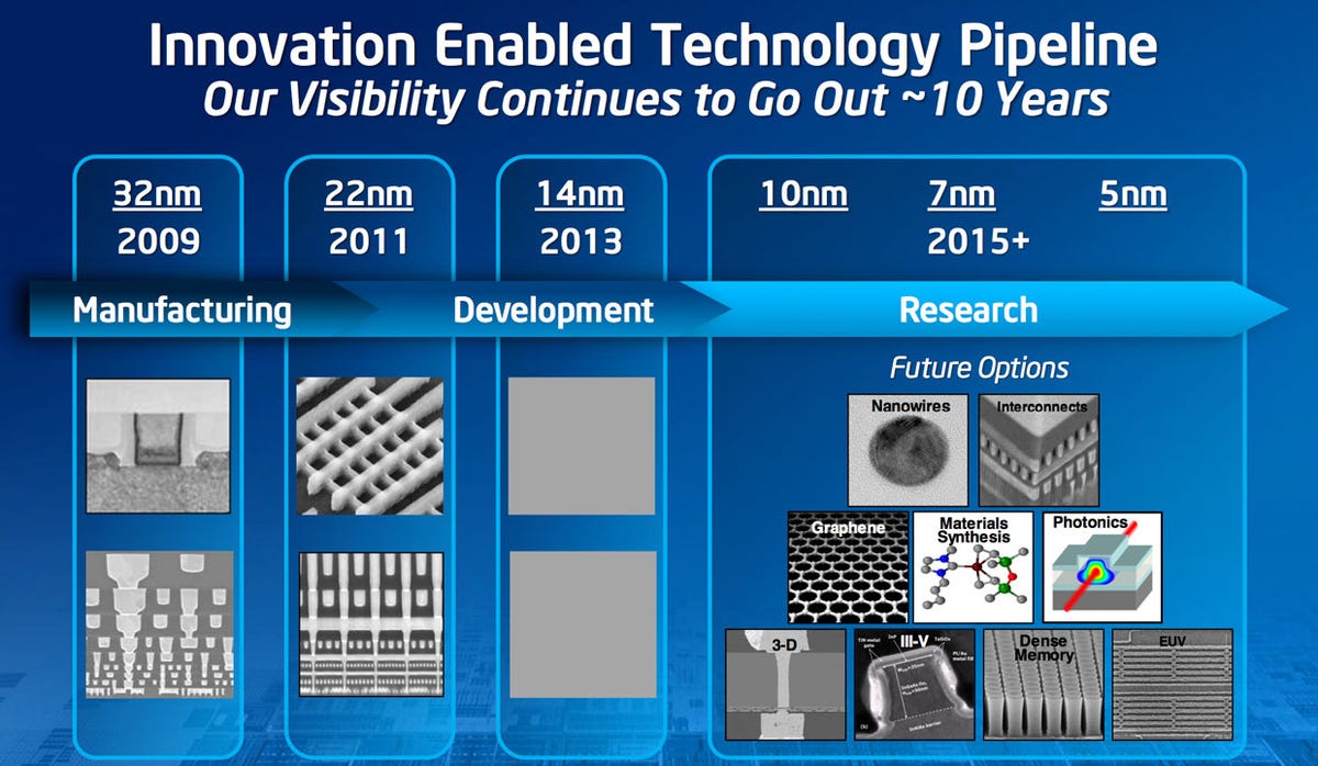
Intel builds its top-end "Ivy Bridge" family of Core chips with a 22 nanometer (22nm) manufacturing process. That means the smallest elements of the chip measure just 22 billionths of a meter, which is to say about 7,500 of them could fit across a dot on the letter i. Each two years, through what Intel calls its "tick-tock" strategy, the chip giant moves to a smaller process that doubles the number of transistors it can pack into a given surface area.
To the market, 22nm chips are new. To Mayberry, they're old hat. He lives in the future, testing new processes to figure out how to scale manufacturing processes down to 5nm -- and what to do after that.
For related coverage, see why Moore's Law is the rule that really matters in tech and what would happen if Moore's Law fizzled.
CNET News' Stephen Shankland talked to Mayberry as part of an in-depth look at Moore's Law today.
Shankland: A lot rests on Moore's Law -- not just the computing industry but also others who depend on computers. Do you lose sleep over the issue of keeping Moore's Law going?
Mayberry: The answer is no. But there's a longer answer. I get asked a similar question: What are the one or two things that keep you up at night? I don't have the luxury of worrying about one or two things. We have to worry about progressive improvements in a lot of different areas. You parse them out, assign them to people, you have competent people working on these things. So I don't really lose sleep over it.
I've heard the end is coming for many, many years, and it's never true. It's my job to make sure it never comes true.
Shankland: I remember times when people predicted this or that manufacturing process would be the end of the line, like at 180 nanometers. How many times have you heard people say something will halt Moore's Law?

Mayberry: I've been at Intel 28 years. I've been hearing about the end of Moore's Law for 28 years.
I probably get contacted by a reporter two to three times a year because they read something predicts the end of Moore's Law. There's usually a grain of truth in whatever it is they're pointing to, but also there's an unspoken assumption that this will happen. In the case of 0.18 microns [180nm], we were worried about two things. One was the ability to print features, which is lithography. The other one was the problem of short-channel effects. As you make transistors small in their electrical length, they turn on easier, which is good, but they turn off harder, which is bad. All through the end of the 1990s, the worry was leakage power: you have to stop scaling [making transistors smaller] because you couldn't turn devices off without overheating.
We did a lot of work on the depth of the channel. We made channels very shallow, which made them easier to control. That gave an ability to sidestep that issue, at least for awhile. You just push the problem around. The next challenge was gate dielectric leakage, which we solved with high-k [a thin layer between the transistor gate and channel made of a material with a high dielectric constant]. Then gate leakage came around, which we solved with tri-gate.
If you're only using the same technology, then in principle you run into limits. The truth is we've been modifying the technology every five or seven years for 40 years, and there's no end in sight for being able to do that.
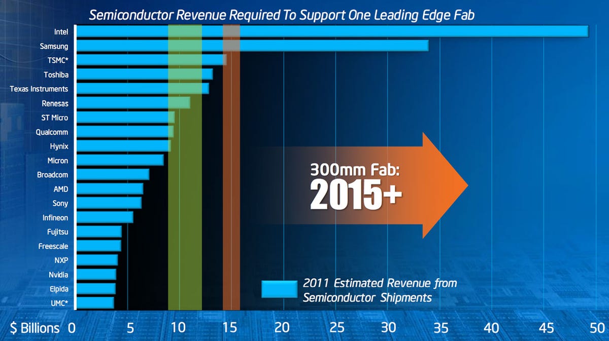
Shankland: Building chips seems like a good business to be in if you're not one of the companies that's getting squeezed out. Intel has survived the steady consolidation. But each new generation of technology requires more R&D funding. Across the industry, does the R&D investment level stay the same, just concentrated in fewer hands?
Mayberry: Let me answer that in pieces. Staying on the leading edge for memory is different for logic technology and different for foundry technology. Looking at the three examples of Intel [which concentrates in logic], Samsung [a leader in memory], and TSMC [Taiwan Semiconductor Manufacturing Corp., the top foundry that makes microprocessors for other companies], the percentage of R&D burden is higher in the memory industry than it is in the other two. That ends up where on average you break even -- in the high part of the cycle you make enough money to make up for the low part of the cycle. It's been that way for a long time.
The economics aren't necessarily a wonderful thing. For the case of logic and foundry, there are more transistors, therefore more wires, therefore more patterning depth, which creates more layers, so the cost of R&D does increase steadily. But if you're able to increase your volume to increase your units, then you're in a steady state. In some cases, where companies have dropped out entirely out and gone to a foundry, it has been because their market hasn't grown fast enough to spread that out.
Generally, it gets harder and therefore more expensive, but the opportunity to sell things also gets larger. From a business opportunity, your market opportunity is expanding at least as fast enough to pay for your R&D.
Shankland: What would happen if Moore's Law came to an end?

Mayberry: There's a flippant answer: the old people would retire and the new people would get new jobs.
Technology doesn't stay the same. People would work on different things. I'm a dedicated buggy-whip manufacturer. I might retire and raise chickens.
We went from bipolar [transistor chip design] to CMOS in the end of the 1980s. There were some designers of bipolar who didn't make that adaptation. The same thing will happen [again]. If we run out of room on a given technology, people will shift to another technology.
If there's no warning, that would be bad. The reality is that we look ahead and therefore prepare for the transition. For people who don't understand how the cycle works, it looks scarier.
Look at automobile manufacturers. First, they delivered something that works at all. Then something people can buy. Then appealing to them in marketing terms. There's been an evolution over 110 years. Our industry is going to evolve, too.
Shankland: What are the nearer-term problems in Moore's Law?
Mayberry: To continue to deliver the expected gains, you can boil it down to about five things. We have to worry about managing leakage [in which electrical current produces too much waste heat, limiting chip speeds]. That means a change to structures, tri-gate being an example. We'll continue down the path of how we do electrostatic control. We know that as we get to smaller dimensions, there's more scattering in the materials and more things that happen because you made things small. Tunneling currents and scattering -- that's an engineering challenge.

Shankland: What's scattering?
Mayberry: If you have a very large wire, the current is in the middle, and you have no issue. As you make the wire smaller, the surface area compared to the bulk gets larger and larger. You get scattering whatever the device -- a wire or transistor -- that effectively can reduce the mobility of the material. We do materials engineering to gain that back.
There are things we're doing related to improving the precision of fabrication. When we get down to the point where we do 1 or 2 atoms, we're certainly in the space of chemistry where you build individual molecules. But there are things in our processes that are equivalent to that. If you can't precisely make the same size device a trillion times on a wafer, then it doesn't make economic sense.
A fourth area is worrying about combining all the requested functions. Do you want to have something that does the radio, that decodes your voice, that does graphics? That SOC [system on a chip] is complicated, but not complicated in the way that just scaling a CPU looks like.
Fifth, we always know we can improve things, but we know we always need something else. There are lots of proposals out there, but there's not a clear winner or loser. We have to evaluate a much broader range of things that we looked at before. What are the right things to look at to make them ready, when we need them?
Shankland: So for number five, you're talking about a post-silicon future?
Mayberry: There are proposed devices that function differently from what we're used to. Different might be better, or it might not be better. It might require inventions in nine other areas to take advantage of it. There are technologies based on magnetism to communicate information [spintronics], but a spin wave travels at a slower rate than an electron wave. If it's slower, how do you take advantage of it? You have to do the wiring differently, the lithography differently, you have to have invention over a lot of different areas.
Shankland: What are the other candidates for moving beyond today's chip technologies?
Mayberry: There are devices based on quantum effects. Devices today already have quantum effects, but they're not not quantum devices. Tunneling, for example, is leakage [a big problem when miniaturizing chips today]. There are proposed devices that rely on tunneling for them to work. The goal there is to try to find something more energy efficient.
In the case of magnetism, those are potential nonvolatile technologies [memory systems that store data without needing a constant power supply]. When they're off, they remember their state, then they can resume. That's potentially more suitable for battery operated devices, but not necessarily something you're interested in up in the cloud.
Other quantum devices are predicted, but people need to go verify they behave the way the theory says. If you put two layers of graphene close together, you get an interesting state. By triggering voltage, you can turn it on and off. In theory, that's a switch. But they haven't demonstrated the way the devices functions in the way they predicted.
There's been an industry consortium called the Nanoelectronics Research Initiative running about six years looking beyond CMOS devices. There are something like 18 different candidates they're keeping track of. There's no clear winner, but there are emerging distinctive trends that will help guide future research.
Shankland: How many more nodes do we have with CMOS chips? How many times can we shrink the process down?
Mayberry: Somebody who's busy ramping the 22nm node says, "Boy this is hard, and the next one is harder." But the 22nm node for somebody in research -- wow, that was two or three generations ago.

My group is in the process of handing off what will be our 10nm node, which is the 2015 process. One of the focus items is the basic architecture for the 2017 node, and there are people looking ahead to the 2019 node. At least through that period of time, we have a decent sense of what it will look like. We will almost certainly make changes on the way. We won't be beyond the end of visibility until at least 2019.
From a naming point of view, that would end up being the 5nm node.
Shankland: Is Moore's Law now a self-fulfilling prophecy, where the industry actually controls the pace -- something planned as opposed to something observed?
Mayberry: That is true. It is first an observation. The original observation was a 12-month cycle. Then it turned into an expectation. The fact that Intel is running on two-year cycles has as much to do with the need to sync the design side with process side than with any reason to pick that date. If the designers couldn't keep up , then we would alter the schedule.
We've gone slower at some points, then faster. From the design of CPU, we have to keep a cadence because the design takes a long time to get done.
Shankland: In the last decade the chip industry hit a power wall, when chip clock frequencies couldn't be increased without drastically increasing power consumption and waste heat. That led to all the multicore designs we see today. Did that shift some of the problem of chip progress to software, where programmers have to deal with parallel programming now?
Mayberry: There was a power wall in the 1980s, a power wall in the late 1990s, a power wall in the middle of the 2000s, which is what you're referring to. If you look at the underlying transistor, we continued to scale the power, and it's a steady curve. It's a matter of what you have to pay attention to. When we went to the Pentium Pro architecture [Intel's first server processor, introduced in 1995], we went to parallelism inside the core. We hid it from the people who had to write the software. We've gone to parallelism a long time ago in the early 1990s. We've now reached point where we need to make the coding of the parallelism more explicit.
One way to do it is do vector processing. That's effectively what the old supercomputers did. Modern GPUs [graphics processing units] in some sense are doing vector processing. That requires a style of how you construct the workload. Some workloads don't work well for that architecture, and other things are laughably parallel. Drawing pixels is very easy to make massively parallel -- that's why we do GPUs for that. When you get into something like modeling weather, you have an element of vector computing, but there is an interconnectedness where each chunk of weather connects the next neighbor, so you need information passed to other computing elements. That's a harder challenge to keep in your head. Somebody who knows how to write Java isn't trained to think in those terms. But we're coming up with tools to think in parallel naturally. We shifted to how we do compilers and you write the code in the first place.
Shankland: Is there a comparably difficult computer challenge the industry has overcome in the past?
Mayberry: Yes. Every problem is different. If you're writing apps for cell phone and expect to be paid 99 cents, you're not going to devote as much energy into optimizing the last bit of performance, so you have to find developer tools to make that easier. If you're writing something that runs in the cloud and executes many times a day, you throw resources into making it run it run more efficiently.
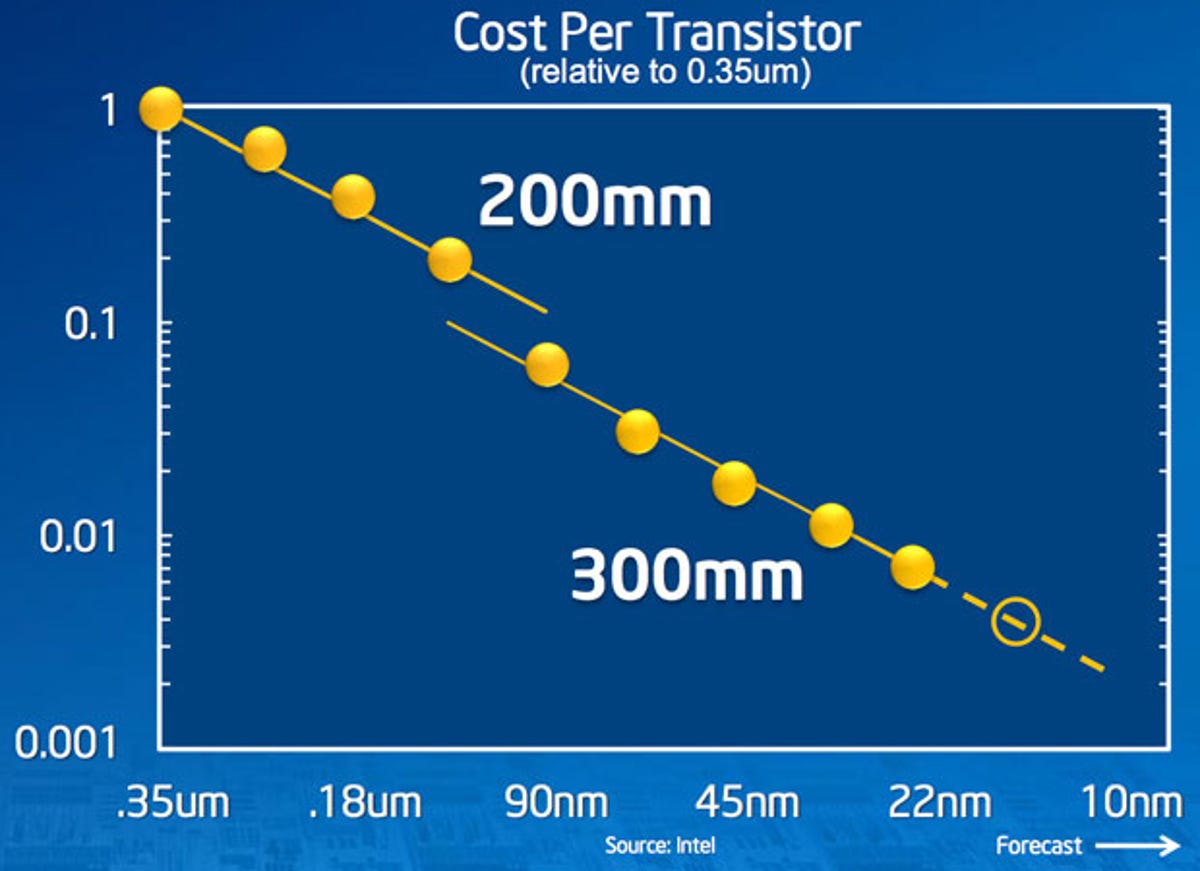
Shankland: One way to get more profit from a given manufacturing process is to increase the size of the silicon wafer on which chips are printed -- the cost of sending a wafer through the manufacturing process stays about the same but you can carve more chips from a larger wafer. We've gone through the 300mm wafer transition. When do wafers move to 450mm in diameter?
Mayberry: This will be the longest time between transitions we've ever had. The 300mm transition was a little over a decade ago. It didn't happen as predicted. There was a lot of uncertainty. The same thing is happening with 450mm.
It'll probably take longer than from 200mm to 300mm, and from 100mm to 200mm, and from when I was a little engineer, from 3-inch to 4-inch. Moore's Law is about economics. If you build more things at the same time, the cost of an individual transistor is less. Building a larger wafer is an economic part. You're building more things at the same time. If you break down the history of how much economic gains we get from scaling [decreasing the size of electronics elements on the chip] and how much we get from increasing wafer size, there is non-negligible amount from wafer size. It might be 80 percent from scaling, but 20 percent from wafer size.
Shankland: Because you get more die [chips] per wafer?
Mayberry: As you make a wafer, you do the same steps at the same time. The cost per step don't go up as much as the cost per wafer. It's like running a larger batch of cookies through the oven. You don't gain as much as you do by shrinking things, but you do gain. I said 80-20 -- that's not the actual number. But it's an important part of the industry long-term.

Shankland: What's your best bet when the 450mm transition will happen?
Mayberry: I think it'll happen in the second half of this decade, between 2015 and 2020. I know we have some targets. Whether they end up being achievable is beyond our control. It's an industry consensus on timing.
Shankland: How hard is it to make a pure silicon wafer that's 50 percent wider?
Mayberry: Basically, you're growing an ingot, then slicing an ingot up into wafers. You start with a small seed crystal, then grow up like a cone to get to the desired diameter, then you end up with a vertical cylinder. You slice off the ends. When you do 50 percent larger wafer size, ... the ingot weighs maybe 3 times more. With the larger weight, you need a larger machine to handle it. When you slice the wafer, you need longer saw blades.
From an economic point of view, you hope that blended mixture ends up being more cost-effective. You get something like a little over twice the area and spend something like 30 to 40 percent more to do that. [Chipmaking equipment] suppliers who do that want to get ahead [of competitors], too. Who pays for the R&D? Do you pay up front? Do you pay at the end? How do we form a consensus around how people foot the bill and how people reap the reward?
Shankland: With smaller chips, we've seen processors move from supercomputers to minicomputers to personal computers to cell phones. Will this continue to the point where, as Ray Kurzweil predicts, we'll have nanobots swimming in our bloodstreams?
Mayberry: There's more computing available in a smartphone than NASA had for a moonshot. The demands for computation are going up as well. In old, old days, you'd submit a deck of punched cards. Now you talk to your device and it sort of figures out what you want to do. That latter task requires a lot of computation. If you offload that to the cloud, it just shifts that problem around. The demand continues to get higher and higher and higher.
The second part is how do you deliver that computation. There's a limit where people can't type on a screen size -- you have to squint to see it. So a device that reads your thought waves? If you look out 20 or 30 years, it's not inconceivable somebody could do that. There's a lot of work in neurobiology trying to figure out what's going on in your head. You get pretty fuzzy results, but computation continues to improve.
I sort of doubt you'll inject things into your bloodstream any time soon. But having something you wear on your head, that might happen sooner. Google glasses is one of the projects where people are looking -- are there different ways to deliver information? Those might happen sooner. How do you deliver something without interfering with the life of a person?
There's that third element of how do you deliver information, taking into account the context you're delivering it. That's a part of perceptual computing, responsive computing, adaptive computing, where you're not only doing from computational point of view the task requested, but the delivery of the information is modified by the context around it. Obnoxious ringtones are funny in the right audience. It would be nice if a phone could figure out "This is appropriate, this is not appropriate."
Shankland: Kurzweil predicts the singularity will happen when Moore's Law makes computing cheap enough for artificial intelligence. Then we can't predict the future anymore. Do you give credence to that idea?
Mayberry: I probably have a more measured view of things. I have always had limited visibility. [In the near future, things are] going to look like today but better. If you look further, we'll have to make a change, but until we get the invention done, I don't know exactly what that is.
One aspect of the singularity is that we can't see past the singularity because we haven't done the inventions yet. The other part is machines that are going to overtake our way of thinking. That's been predicted for a long time, and it's never happened. I'm a little skeptical we can say that a certain point it's going to happen.
Shankland: The number of chipmakers is steadily shrinking. Where does the consolidation end? With one giant organization?
Mayberry: I don't think we can predict that. We don't do all our R&D by ourselves. We rely on the R&D at our tools suppliers and at our materials suppliers. We engage universities. The ecosystem is much broader than the headline of the numbers of the company that ships the final thing.