Adios, silicon: Why exotic designs are the future for the chips in your gadgets
Decades of progress creating conventional computer chips will stall in the coming years, forcing some far-out ideas on semiconductor makers. Carbon nanotubes or quantum computing, anyone?


- Shankland covered the tech industry for more than 25 years and was a science writer for five years before that. He has deep expertise in microprocessors, digital photography, computer hardware and software, internet standards, web technology, and more.
Most of us assume that smartphones and laptops will keep getting faster and better.
But that progress could come to an end in about a decade.
That's when engineers will hit the limits of cramming atom-scale circuitry onto conventional silicon chips, the brains behind every computing device today. That means the iPhone 11 you get in 2024 will be about as good as it gets.

Ho-hum, you might say. But the problem is much deeper than lackluster new gadgets. Chip advances have powered one technology revolution after another: PCs, the Internet, smartphones, smartwatches and, soon, self-driving cars.
Fortunately, the chip industry, led by market leaders Intel and Samsung, has plenty of ideas for getting around that impasse. Those plans begin with refinements to today's technology and grow steadily more exotic. Look ahead, and computers could fit inside your contact lenses or swim in your bloodstream.
It's not clear which ideas will prevail yet, but the end of computing history will not come when today's silicon chip technology runs out of steam.
"It's the equivalent of a turn, not a step off a cliff," said Mike Mayberry, manager of Intel's components research. Mayberry's job is to look as far as 15 years into the future to chart Intel's course from today's tech to something dramatically different.
Tiny circuits
The fundamental element of a circuit is called a transistor -- a tiny on-off switch that governs the flow of electrical current. Transistors are linked in complicated cascades called logic circuits in which the number 1 represents flowing electrical current and 0 represents no current. Those transistors work together to ensure you can quickly pull up your Instagram app for a well-timed selfie.

Conceptually, the transistor has been the same since Frank Wanlass patented the design in 1963. But physically, it's changed dramatically -- shrinking so much that Intel's Xeon server chips, released in 2014, are packed with 4.3 billion transistors.
It's the result of Moore's Law, the steady cadence of chip improvement first observed in 1965 by Intel co-founder Gordon Moore, who noted that the number of on-chip transistors doubles, on average, every two years.
The problem is that in a decade or so, transistors won't be able to shrink further because their components will be only a few atoms in size. You can't make things out of half atoms.
Fortunately, there are other ways to improve chips without doubling their circuitry.
How? One approach would be to stack today's flat chips in layers -- like fitting more people into Manhattan by building skyscrapers rather than one-story offices. Chips could also progress by getting more work done in a given amount of time. Or they might work more like human brains, which run on chemical fuel and rely on billions of neurons working together in parallel.
Innovation requires a lot of engineering and materials research at universities and company labs, propelled by the $336 billion chip industry.
Bigger challenges
Industries measure progress with numbers like horsepower for cars or crop yield for farming. In the chip business, the number is linked to the size of part of the transistor measured in nanometers -- billionths of a meter. Intel and Samsung today use a process in which more than 10,000 transistors could fit on the side of a red blood cell that's about 7,000nm in diameter. By comparison, a sheet of paper or human hair is about 100,000 nanometers thick.
Skip ahead four generations of that miniaturization process, and 160,000 transistors would fit on that same red blood cell.
That is, if the industry can keep pace with Moore's Law. Each new step -- or node -- is getting more technically difficult and more expensive.
"For the last 50-odd years, it's always been true that whenever you go to smaller nodes everything gets better," said Scott McGregor, chief executive of communications chipmaker Broadcom. "It's no longer true. For the first time, per-transistor cost is now starting to go up."
Rising costs could definitely slow computing advances -- unless you're willing to pay a premium, that is. "To make it smaller and faster, you're losing the cheaper part of the game," said Michael Jackson, associate professor of microelectronic engineering at the Rochester Institute of Technology. "Do you want to see the price of a cell phone go back up to $2,000?"
No, you don't, and neither does anyone else. That's why chip researchers will push into new directions -- starting with modifications to the silicon itself.
Adding new materials
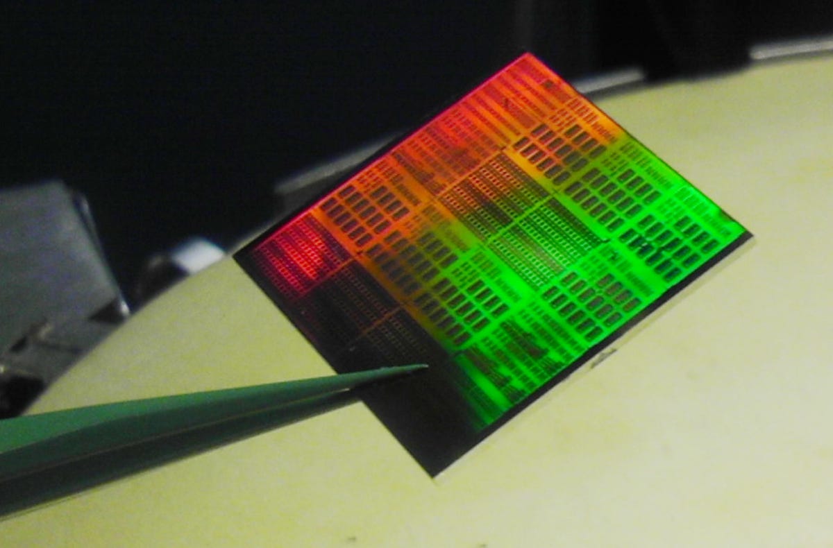
Today's chips are made from silicon wafers 300mm (12 inches) in diameter and less than 1mm thick. Each circular slice of silicon crystal is transformed by many steps -- layered with coatings, zapped with carefully patterned light, bathed in solvents, implanted with electrically charged atoms called ions -- until it houses an array of identical rectangular chips. Through careful cutting, the wafer is diced up into individual chips.
Why start with a circular wafer if you're making rectangular chips? Because it's easier to grow the near-perfect silicon crystals in a cylindrical shape, and the cylinder is sliced into the wafers.
Silicon falls into what the chip industry calls group IV of the periodic table of the elements. One way to keep pushing progress will involve elements drawn from columns to either side of the group IV column -- thus the term III-V materials, pronounced simply "three-five."
With III-V chip manufacturing, all that stays the same -- but silicon will get new elements layered on top. That will help electrons flow faster, which means less voltage needed to get them moving. If the chips need less power, then transistors can be smaller and switch faster.
One company betting its future on III-V materials is Efficient Power Conversion, a 34-person startup led by Chief Executive Alex Lidow. EPC already is seeing steady revenue growth from devices that incorporate a III-V layer made of gallium nitride (GaN). In 2016 or 2017 he expects to adapt the gallium nitride manufacturing process to work for the logic circuits that do the thinking in computer processors. Because of gallium nitride's electrical properties, "you immediately get a thousand times potential in improvement" over conventional silicon, he said.
Crazy carbon
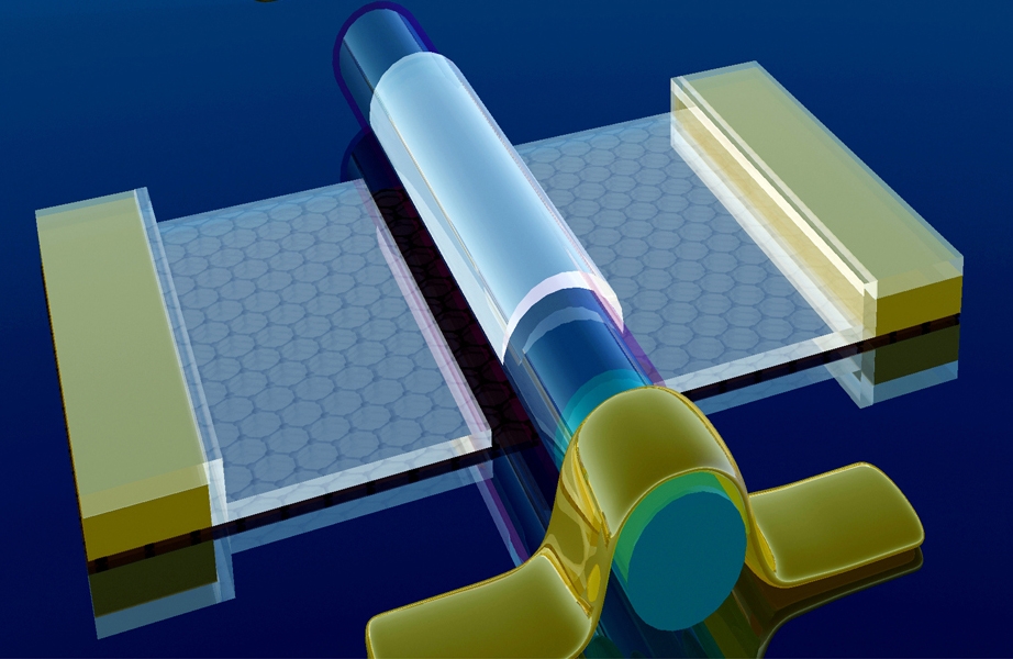
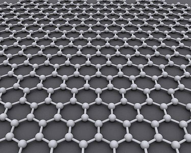
IBM is investing big in exotic forms of carbon as a way to recraft chips. Graphene, for example, is a sheet of carbon atoms just a single atomic layer think, arranged in a hexagonal array that looks like a chickenwire fencing. Another is carbon nanotubes, which are like tiny straws made from rolled up graphene sheets.
Both forms of carbon could help push miniaturization further than what's possible with conventional silicon. And processors could get faster even if they don't get smaller -- a big selling point.
Nanotubes could become transistor building blocks, although placing them precisely is a big challenge, said Supratik Guha, director of Physical Sciences at IBM Research. He believes the tiny tubes could find their way into processors two or three generations out.
Both nanotubes and graphene present challenges. Nanotubes, for example, are 99.99 percent pure but IBM needs to improve that by a factor of 10 or 100, Guha said.
Graphene is "the wonder material, but it's a lousy transistor," Intel's Mayberry said. But because it shows promise, Intel is researching ways to improve graphene's semiconductor properties so it'll work on chips.
Further out: spintronics?
Spintronics is a more radical approach.
Conventional electronics process information based on electrons' negative charge. But the industry has long been interested in using electron particles' spin --conceptually akin to how a planet can rotate clockwise or counterclockwise on its axis -- to process information. You can't see an electron's spin, but you can influence and measure it with a magnetic field. Different spin directions can be represented by the 1s and 0s at the foundation of digital computation.
Spintronics' big potential advantage is energy efficiency -- an important edge because power consumption and heat limit how fast today's silicon chips can run.
Srini Banna, director of technology development research at GlobalFoundries, is a fan because, in his view, spin-based computers could beat those based on carbon nanotubes to market. Here, too, there are challenges. For example, a computer would use spintronics within its deepest interior but rely on traditional electronics further out to communicate with memory, drives and networks. Translating data and instructions between the two zones takes time.
That's a concern for IBM's Guha. "I don't believe spintronics will be a drop-in replacement for silicon," he said. Still, it could be useful in things like remote sensors that don't need fast processing but do need very low power consumption.
Quantum computing
Quantum computing just might be the most mind-bending idea out there. The field explores physics phenomena at ultra-small distances that are profoundly different from what humans experience.
Here's one example of that weirdness. When we flip a coin, it lands as either heads or tails, which in computing terms is described by either 0 or 1. But quantum computers use "qubits" -- quantum bits -- that can be both 0 and 1 at the same time through a quantum mechanics concept called superposition.
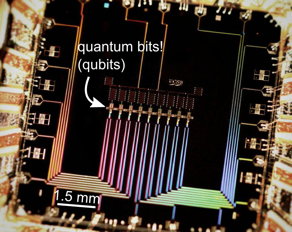
Qubits are core to the advantage of quantum computers, said John Martinis, who leads much of Google's quantum computing work. Because qubits can represent data in multiple states at the same time, they can be used to explore multiple solutions to a problem at the same time. In other words, quantum computers can test lots of possibilities in parallel instead of testing one after another the way a conventional computer chip does. Each time you add a new qubit to a quantum computer, you can try twice the number of solutions.
"You can do so much more than you can do with a classical processor," Martinis said, though quantum computers must be kept extraordinarily cold to keep the qubits still enough to do their processing magic.
Google thinks quantum computers will boost particularly complex computing chores like image recognition, speech recognition and language translation. But there's a catch: "The vast majority of workloads in the world are still better off on conventional computing," Mayberry said.
There are a lot of other promising technologies out there, too. Silicon photonics could shuttle data around a computer faster, while re-engineered DNA might enable living cells to perform computation. That wouldn't replace a smartphone chip, but it could expand computing technology to new realms like medical diagnosis and treatment.
All these ideas could help the industry continue its pace of nonstop innovation even after silicon-based chips hit their limit.
"Think of a flock of birds," said IBM's Guha. "When the lead bird tires, it moves to the back, and another bird takes the lead. Moore's Law has carried us fantastically the past 30 or 40 years. I'm not worried that the flock of birds won't keep going."
Correction, 7:40 a.m. PT April 20: The spelling of Srini Banna's name has been fixed.