IBM tips into microscopic manufacturing
Fabrication is moving to the nanoscale, aided by a super-hard tip 10,000 times smaller than a pencil point that could be used for microscopic biosensors and optical probes.


A team of researchers have designed a material durable enough to operate on a microscopically small scale, a step toward fabricating nanoscale biosensors and optical equipment.
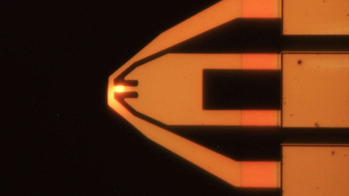
IBM Zurich today announced the results of a collaboration with the University of Pennsylvania and the University of Wisconsin-Madison to build an ultra-small probe tip, which is 10,000 times smaller than a pencil point. Because it's substantially harder than previous designs, it's hard enough to be a component in microscopic mechanical machines.
For example, these tips could be part of in-body monitors to track glucose levels in diabetic patients or sensors to measure water pollutants.
Typically, tips made from silicon, which are measured in microns, wear out quickly or are unstable at high temperatures, the research said in a paper published today in Advanced Functional Materials. But to make biological or environmental sensors, devices need to be durable and have other desirable properties, such as being chemically inert and a good conductor of heat.
The researchers turned to a metallurgy process called annealing, used to harden steel, to produce a tip using silicon carbide that's 100 times harder than a previous tip the group made out of silicon oxide-doped, diamond-like tips. The method allows for a durable coating to be applied to the underlying material without changing the original shape.
With this material, manufacturers can start to make devices, such as sensors or probes used in nanoscale lithography, data storage, or thermal imaging, according to the paper. "This is a significant achievement that will make nanomanufacturing both practical and affordable," University of Pennsylvania professor Robert Carpick said in a statement.