Want a smarter phone? IBM and Samsung bring you: Nanosheets!
Big Blue's research alliance to shrink computer chips develops technology to boost performance by 40 percent over today's processors.


- Shankland covered the tech industry for more than 25 years and was a science writer for five years before that. He has deep expertise in microprocessors, digital photography, computer hardware and software, internet standards, web technology, and more.
IBM, Samsung and GlobalFoundries use technology called nanosheets to make computer chip circuitry even smaller.
If you're frustrated that your smartwatch isn't that smart or your phone doesn't pack enough power, IBM and Samsung have some good news for you.
The allies have announced a technology they call nanosheets that should help shrink chip electronics by another notch, a move that's necessary to squeeze more computing power into a smaller processor. Compared with today's chips, they expect a 40 percent performance boost at the same level of power consumption or, alternatively, the same performance but using only a quarter the power.
The development is important, as chipmakers for decades have driven progress in the technology industry, with miniaturization that enabled first personal computers and then powerful phones . But it's been hard to maintain the rate of progress, charted by Moore's Law, that for years meant a steady doubling every two years of the number of tiny switches called transistors that would fit on a chip. Even chipmaking powerhouse Intel, whose co-founder Gordon Moore came up with Moore's Law, has slowed down its cadence.
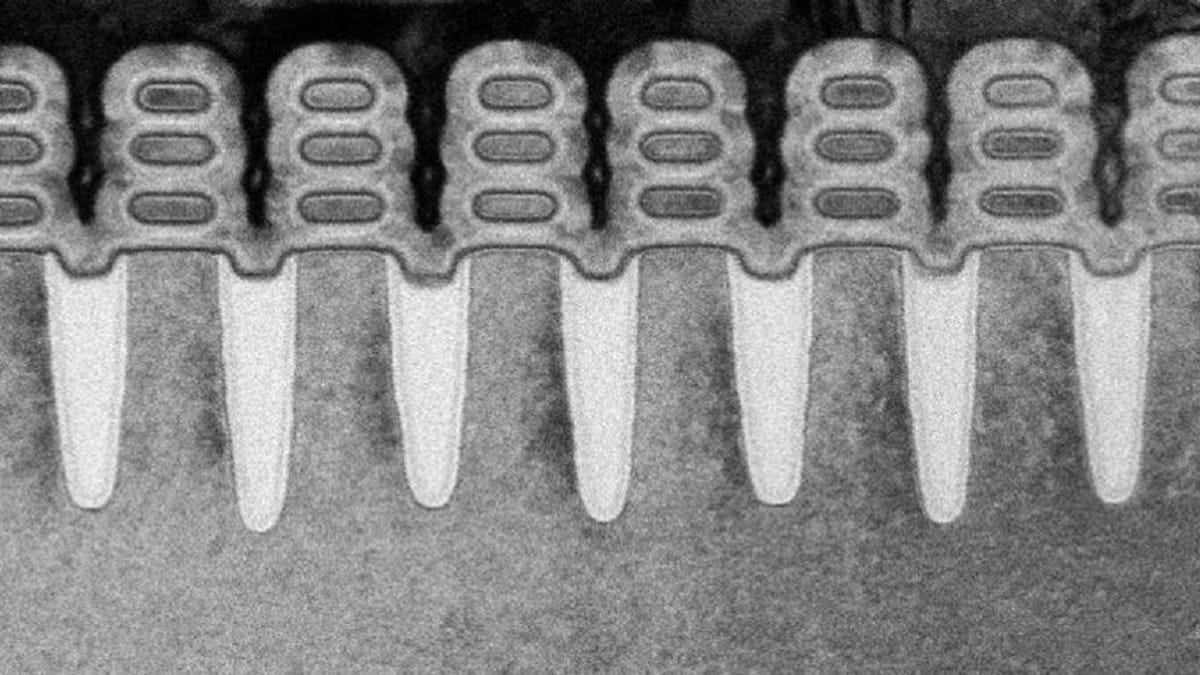
Today's chips are built with transistors whose dimensions measure 10 nanometers, which means about 1,000 fit end-to-end across the diameter of a human hair. The next generation will shrink that dimension to 7nm, and the IBM-Samsung development goes one generation beyond that to 5nm.
Chips with more brains
That means transistors can be packed four times as densely on a chip compared with today's technology. All that circuitry can help computing jobs like combining multiple photos into a single panorama, recognizing a voice command or stabilizing shaky videos.
"A nanosheet-based 5nm chip will deliver performance and power, together with density," said Huiming Bu, IBM's director of silicon integration and device research.
Take all those numbers with a nanograin of salt, though, because chipmakers no longer agree on what exactly they're measuring about transistors. And there's also a long road between this research announcement and actual commercial manufacturing. IBM believes this new process won't cost any more than chips with today's transistor designs, but its approach requires an expensive shift that chipmakers have put off for years: the use of extreme ultraviolet light to etch chip features onto silicon wafers.
The IBM research alliance with Samsung and chipmaker GlobalFoundries disclosed the development Monday at a Japanese processor conference.
More transistors
Chips in phones and PCs today offer billions of transistors, switches that start and stop the flow of electrical current millions of times a second. Those carefully orchestrated flows of electricity are how a computer chip performs operations like adding two numbers together or noticing that some data just arrived over your Wi-Fi network.
A key part of transistor design is called a gate, the element that's responsible for shutting off current or letting it flow. For decades, transistors were flat and gates perched on top of the channel through which current flows. To shrink transistors further, chipmakers moved to a finlike design that makes the channel sprout up vertically from the substrate. The gate is draped across the top of the fin.
To shrink the chips further, IBM and Samsung had to come up with a way to improve contact between the gate and channel even more. The end result is nanosheets, which provides a way for the gate to completely surround the channel, Bu said. Multiple fully enveloped channels run side by side in parallel for each transistor.
It all sounds pretty good. Just don't hold your breath. "Mass manufacturing could happen within a few years," Bu said. So this decade, we'll have to make do with less dramatic improvements to our phone hardware.
CNET Magazine: Check out a sample of the stories in CNET's newsstand edition.
Crowd Control: A crowdsourced science fiction novel written by CNET readers.