IBM nanosheets promise better speed and battery life for next-gen chips
The processor performance improvements could come in 2024 or 2025 -- if IBM finds manufacturers that'll license its approach.


- Shankland covered the tech industry for more than 25 years and was a science writer for five years before that. He has deep expertise in microprocessors, digital photography, computer hardware and software, internet standards, web technology, and more.
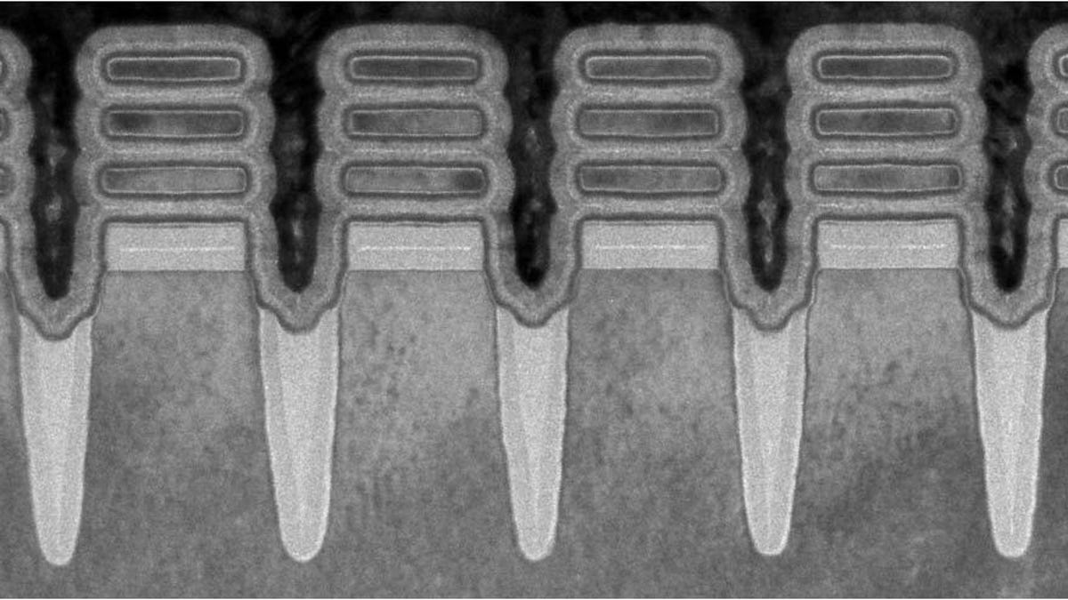
This photo shows a cross section of six transistors built with IBM's nanosheet technology. Each has a stack of three nanosheets that carry electrical current. And with an approach called gate-all-around, each nanosheet is surrounded completely by a gate, the transistor component that switches current off and on. Today's chips process data using billions of such transistors.
IBM Research has developed new chipmaking technology it says will advance processors to the next level of circuitry miniaturization, performance improvement and power efficiency. But to make this real, it'll have to find manufacturing partners to bring the tech to market.
The new manufacturing technology, featuring components called nanosheets, increases chip performance 45% or reduces power consumption by 75% compared with the one used to make IBM server chips or Apple's iPhone chips, IBM said Thursday. The company expects the technology to arrive in processors in 2024 or 2025, two generations beyond the most advanced processes currently used by today's manufacturing leader Taiwan Semiconductor Manufacturing, or TSMC.
The same basic chipmaking technology that's been used for decades underlies IBM's approach: a carefully arranged pattern of light beamed onto silicon wafers to etch patterns that become the data-processing circuitry elements called transistors. Continuous refinements have let chipmakers gradually shrink those transistors so that processors once used in room-size mainframes can now power a smartwatch.
The new method uses two structures. The first are nanosheets, the thin, flat wires that carry electrical current across the transistor. Second is a new design for the gate, the transistor component that switches that current on or off. IBM uses gate-all-around technology that completely surrounds each nanosheet with the gate material to keep electrical current from leaking.
"We have the transistor device to make it happen, and we are seeing the performance improvements," said Dario Gil, head of IBM Research, which licenses its chip technology for manufacturers to use. "The entire industry is going to use this transistor technology."
Chip progress is important. Cutting power usage is critical for battery-limited mobile devices, as well as improving performance makes apps faster and more powerful. Shrinking transistors means more circuitry for faster graphics, AI processing and other dedicated hardware abilities.
2nm manufacturing process
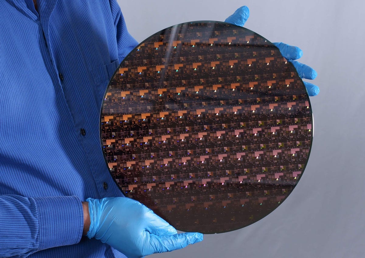
The company on Thursday showed off silicon wafers studded with rectangular chips using the new approach. IBM Research is building the test chips at its semiconductor research facility in Albany, New York, a choice that will likely sit well with politicians eager to restore US chipmaking prowess.
Chipmakers refer to their manufacturing processes by the super-small dimension of nanometers, a billionth of a meter. A strand of DNA, for example, is 2nm wide. For chipmaking, a smaller nanometer number indicates progress in miniaturization though the terms used today are largely labels rather than actual measurements.
Today's most advanced manufacturing is TSMC's 5-nanometer process. Much of the industry still uses 7nm or earlier processes. Next in line is 3nm. IBM labels its new process as 2nm. Each step on this path is called a manufacturing node.
Since we're running out of nanometers, it isn't clear what labels will come next, especially since the numbers are no longer true measurements.
Gil suggested that perhaps we'll switch to angstroms -- a unit of measurement that's one tenth of a nanometer. But he laughs about the idea since the label now is divorced from true measurements.
"The number of the node ceased having meaning since 65nm," Gil said. "Ever since then, all it really means is the name of the next node two years later."
Other chipmakers already working on gate-all-around
What isn't clear is how the technology will come to market since IBM no longer makes its own processors.
With a stack of tiny flat wires called nanosheets, IBM Research promises chips with faster, smaller components that use less power.
The world's three major chipmakers -- Intel, TSMC and Samsung -- all have their own research programs and likely already are working on gate-all-around technology, said David Kanter, principal analyst at Real World Insights. "Every major player clearly has plans for this."
Samsung showed off its gate-all-around technology at a February conference, and Intel, like IBM, is working on stacking multiple layers of nanosheets into each transistor.
IBM has partnerships with major chipmakers, though. Samsung builds IBM server processors, and an IBM research alliance is part of new Intel Chief Executive Pat Gelsinger's plan to turn around Intel's years of problems.
Another complication for IBM will be proving its technology works outside of a lab in high-volume manufacturing, where costs and consistency are crucial.
"For semiconductor manufacturing, simply doing the R&D and proving it out is quite a bit different than proving that it scales," Kanter said.