IBM: Faster, not hotter, 32-nanometer chips coming
Big Blue is claiming higher chip performance--but not higher operating temperatures--using next-generation 32-nanometer chip-manufacturing technology.


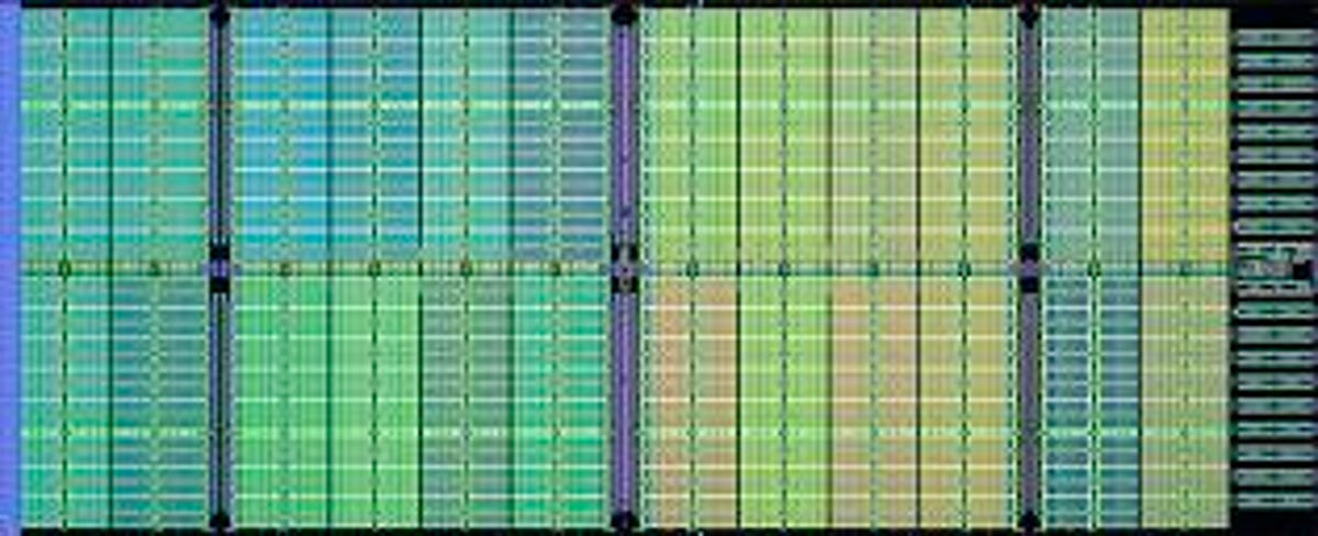
Chips in 2009 will run faster but not necessarily hotter. That's the gist of what IBM, along with its joint development partners such as Samsung Electronics and Toshiba, announced Monday.
The IBM alliance is using "high-k/metal gate" technology to achieve this, the same category of process technology that Intel currently uses in its 45-nanometer processors. The alliance says it is seeing performance improvements of up to 35 percent over 45nm technology at the same "operating voltage" or power levels.
This allows alliance chipmakers such as Samsung, Toshiba, and Freescale Semiconductor (formerly an arm of Motorola) to build more powerful chips that don't necessarily generate more heat. This is a necessary advancement for small devices such as cell phones, as well as data centers that use a large number of servers. The power reduction compared to 45nm technology can range as high as 30 percent to 50 percent, depending on the operating voltage, according to IBM.
The announcement serves as more of a progress update than a breakthrough achievement. At the beginning of last year, IBM announced technology to "speed the implementation of...high-k/metal gate in next-generation 32-nanometer computer chips."
A gate is a basic building block of a digital circuit, while high-k/metal is the material used. Intel, for example, used a high-k material called hafnium to replace the transistor's silicon dioxide gate dielectric for its 45nm processors. As transistors shrink, leakage current can increase. For chipmakers, it is crucial to minimize leakage. This is where high-k/metal gates come into play.
The technology will be available to alliance partners in the second half of 2009, though the design process for devices that use this technology can start now, IBM said. AMD was not included as part of the alliance because technically, it is a member only of a separate alliance, SOI (Silicon-On-Insulator).