What it's like inside a $7 billion Intel fab
The chips are tiny, the manufacturing equipment is huge and the bunny suits are frumpy. Intel wants to build more than a dozen more fabs in coming years.


- Shankland covered the tech industry for more than 25 years and was a science writer for five years before that. He has deep expertise in microprocessors, digital photography, computer hardware and software, internet standards, web technology, and more.
When you walk among the hulking machines inside an Intel chip factory, you feel simultaneously dwarfed and gigantic.
Dwarfed because such factories, called fabs, are enormous facilities covering dozens of acres. And gigantic because the processors they build are often smaller than your pinky fingernail -- the transistors on them are so tiny that thousands could fit side by side across the width of a human hair.
Fabs are the pinnacle of automated manufacturing, the core of Chief Executive Pat Gelsinger's plan to reclaim Intel's chipmaking leadership, and the centerpiece of an effort by the US chip industry and political allies to claw high-tech manufacturing back from China and other Asian nations during a global chip shortage.
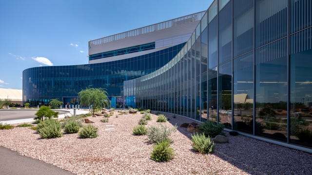
But what are they really like? Are there really people in bunny suits and robotic arms slinging rainbow-colored discs like $10,000 Frisbees? I visited two Intel fabs on a 700-acre plot in the Phoenix suburbs this fall to find out as part of CNET's look at manufacturing in the US.
I learned they're highly automated, excruciatingly expensive and the least dusty places in the state.
From the outside, fabs just look like other huge industrial buildings, surrounded by giant ducts, parking lots and water purification systems. But road signs are a dead giveaway about what's going on: Wafer Way, Angstrom Avenue, Cleanroom Corner, Transistor Terrace, Processor Parkway, Silicon Street. Tick-Tock Trail dampens the fun a bit -- it's named for Intel's old approach toward steady chip progress. But, as I explain in my related feature, when Intel failed spectacularly several years ago, rivals Taiwan Semiconductor Manufacturing Corp. (TSMC) and Samsung were able to pull ahead.
See also: Intel's chip recovery plan could restore US manufacturing prowess
Intel's Fab 42 cost $7 billion when its construction began in 2011. Now these facilities are $10 billion a pop, though Intel hopes US subsidies in possible legislation will knock about $3 billion off the price.
Chip fabs 101
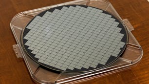
A fab's job is to ingest circular slices of flawless silicon crystal called wafers and, after 500 or so processing steps lasting three months or more, to spit out finished microprocessors. Each chip has billions of electronic on-off switches called transistors that, ticking billions of times a second to the beat of the chip's clock, process data so you can text Dad or see who's ringing your smart doorbell.
One of the hallmarks of fabs is that they are clean. Like, really clean. Any speck of dust or dryer lint will ruin a chip that can sell for hundreds of dollars. Chipmaking operations seal wafers away from the outside world, and the entire fab is under positive air pressure to keep contaminants from blowing in.
To get from one machine to another, plastic modules called FOUPs -- front-opening unified pods -- whisk stacks of wafers around the fab along ceiling-mounted tracks. It's all governed by a central computer system that knows which wafers go where for manufacturing and testing. The black FOUPs whiz by overhead then drop down on cables to disgorge or collect wafers through hatches on each fab machine.
It made the hundreds of robots I saw a few years ago in Volkswagen's factory in Wolfsburg, Germany, look like clumsy, lurching giants. On the other hand, I could see the cars being made. Most of the time, wafers are hidden away, exposed mostly to expensive metrology equipment that scans for defects.
Filthy humans
More precautions are necessary to protect against humans, with our shedding hair and gross dead skin cells. People must seal themselves almost completely inside outfits sometimes called bunny suits that Intel pioneered in 1973. In Fab 42, which makes chips using the new Intel 7 manufacturing process, I had to use two pairs of gloves -- the outer pair was only worn long enough to get dressed, then discarded since it had touched my regular clothes.
I had to swab my camera equipment down before entering the fab, too, and use a special latex cleanroom notebook that sheds less than a hypoallergenic labradoodle.
Despite what you may have learned from Intel's 1997 Super Bowl ad, the bunny suits are not flattering unless you're into the frumpy paper bag look. Special booties ground you electrically -- verified by a test as you enter -- so you don't zap anything with your static charge.
Hair covers, beard covers and a COVID-19 mask completed my transformation into an almost completely anonymous biped recognizable only by my color-coded badge. Plenty of people get used to it, though: Intel employs 12,000 in Arizona and 21,000 at its Oregon fabs.
$150 million machines
There are many chipmaking machines in a fab, but the most prestigious are involved in the process of photolithography -- translated literally, writing on stone with light. Chips are made by shining ultraviolet light through a very carefully designed mask that selectively blocks the light. The wafer, coated ahead of time with a light-sensitive material called photoresist, is chemically altered where the light strikes.
Lithography is a tricky business since the features on chips have shrunk so small and keep on shrinking a little more every couple years. A process called multiple patterning lets chip designers use several illumination steps, each with its own mask, to create one set of structures that's finer than the wavelength of light would otherwise permit. It's so sensitive that fabs are built on geologically stable land and equipment rests on vibration-isolating mounts.
The latest lithography machines, from market leader ASML, cost about $150 million each and blast tiny droplets of tin with lasers to generate ultrahigh frequency light with an ultrashort wavelength. Intel is only beginning to use this extreme ultraviolet lithography process, trailing TSMC and Samsung, but it's one of the pillars of Gelsinger's comeback plan.
The rising expense of this equipment is one reason for Moore's Second Law, which posits that the price of a new fab doubles every four years. Intel's recovery plan involves $20 billion in new Arizona fabs now under construction, billions more to upgrade fabs in New Mexico, Ireland and Israel, and an eye-watering $200 billion to set up two entirely new "megafab" sites in the US and Europe.
After the patterning, wafers are shuttled to another machine that treats the wafer chemically. Areas of photoresist that were illuminated wash away, exposing materials underneath that are then removed with another chemical process called etching. The remaining protective photoresist is then removed with another chemical process, and the entire cycle repeats for another set of structures.
Fabs run 24 hours a day, 365 days a year. Even then, it takes about three months to turn a pristine wafer into a finished product studded with dozens, hundreds or even thousands of rectangular chips.
Packaging chips
A second fab I visited, CH4, specializes in what comes next, packaging. In olden days, that just meant attaching a chip to a circuit board housing and making sure it was protected. Now it often means linking multiple "chiplets" together into a single larger processor.
In Intel's CH4, this different kind of fab work is underway. It's less glamorous than photolithography: "We're the cheap guys. We wear jeans and T-shirts," says Babak Sabi, who leads Intel's packaging development work.
But it's increasingly important. Packaging is getting high tech, enabling ultrafast communication links between multiple chiplets and now letting chipmakers stack them on top of one another in space-saving, high-bandwidth 3D arrangements. It lets designers assemble a processor by combining fast, expensive chiplets with slower, cheaper ones that don't require cutting-edge performance, too.
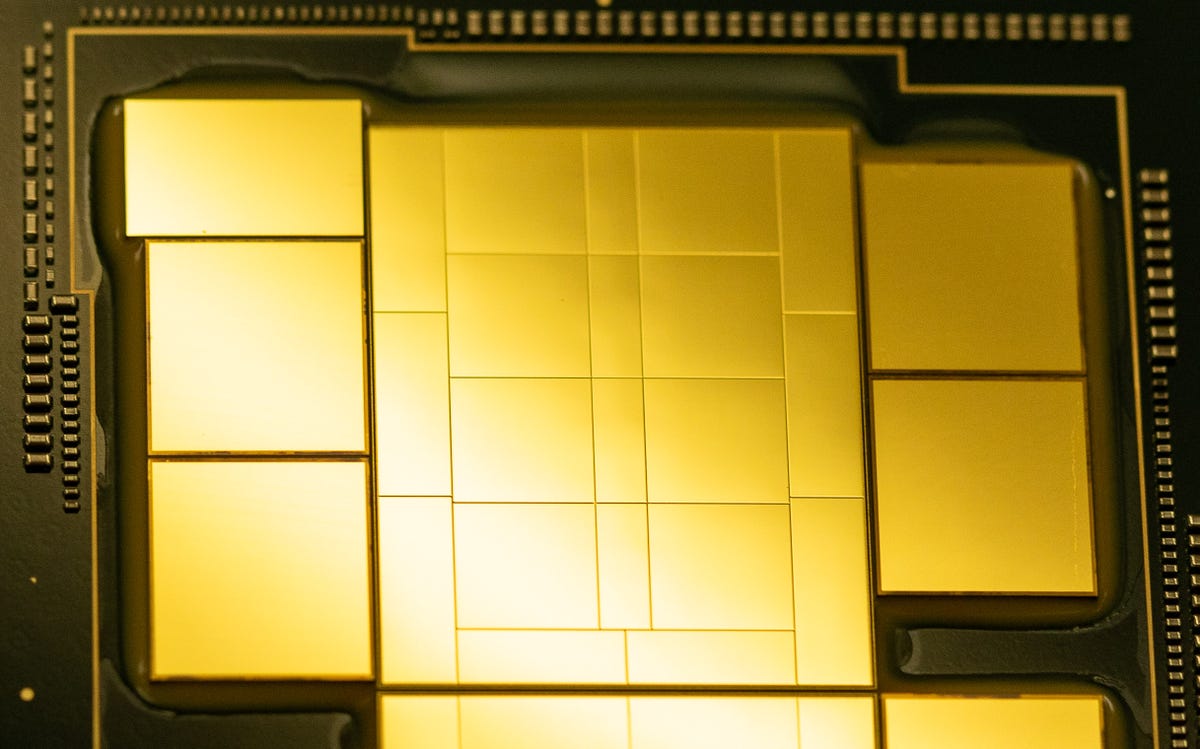
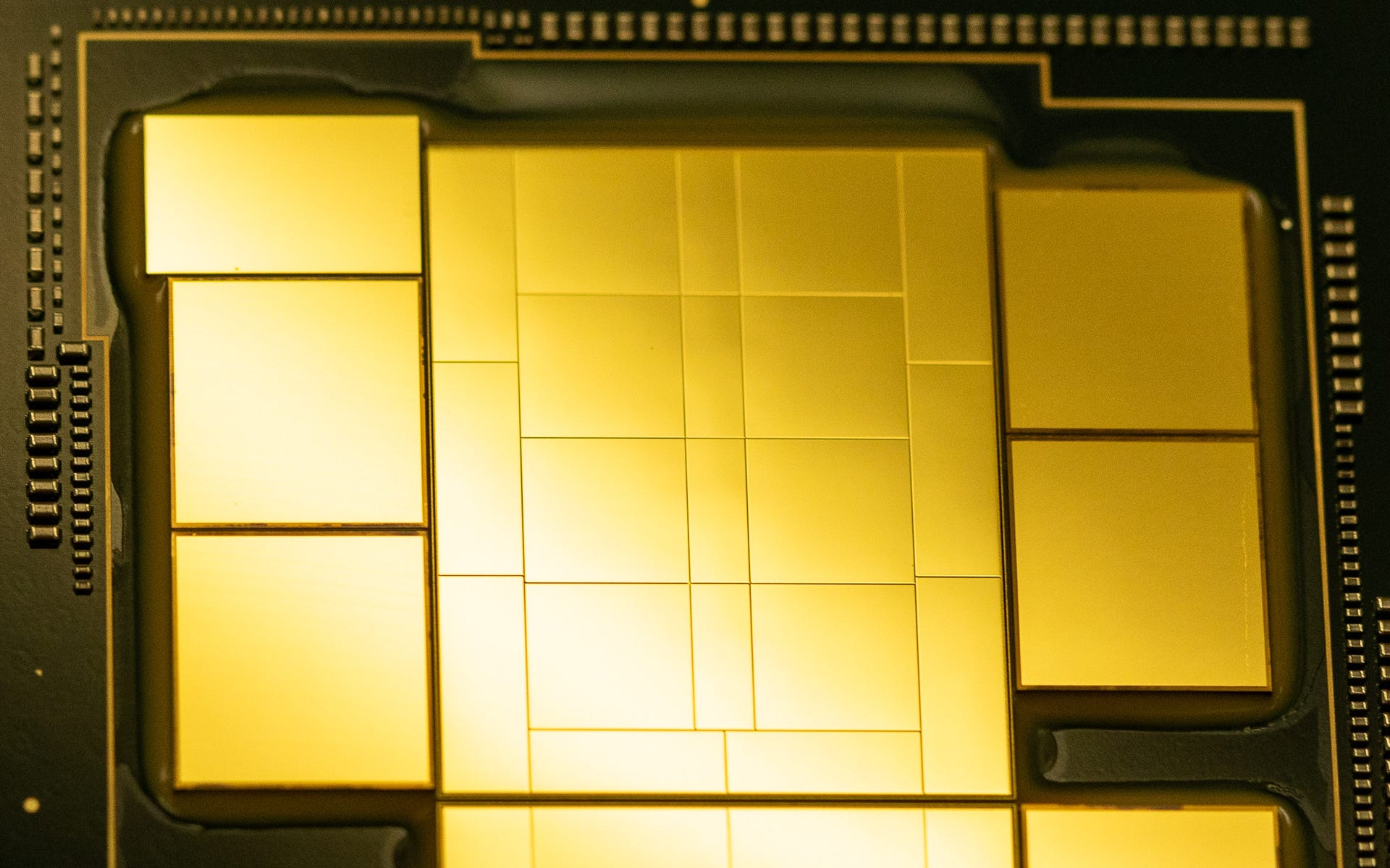
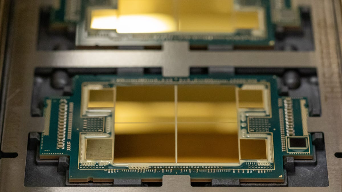
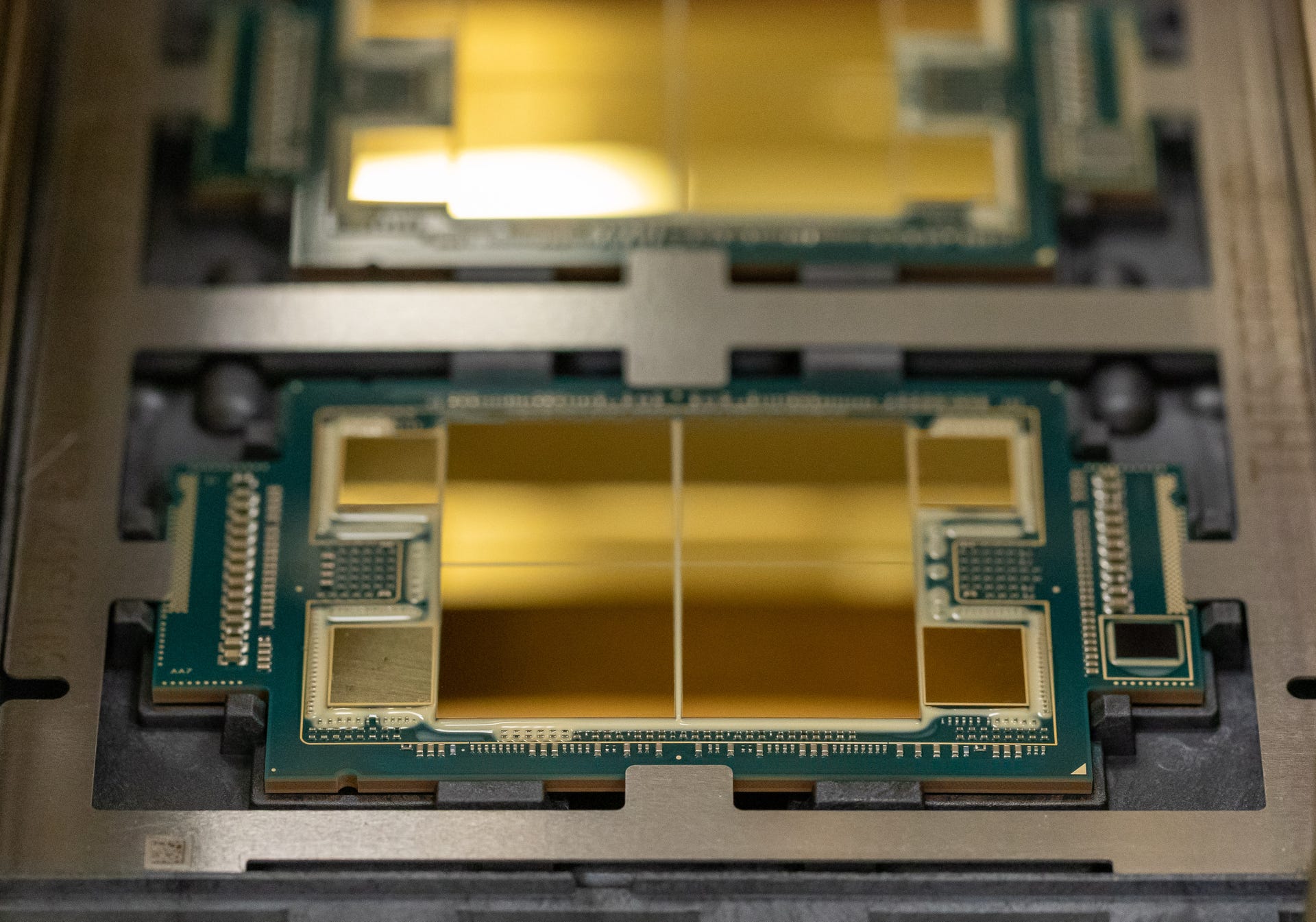
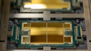
Intel's Ponte Vecchio processor is a packaging tour de force that combines 47 separate active silicon elements, linked horizontally and stacked vertically. This view shows just half of one of the billion-transistor processors.
From CH4, an Intel plane shuttles chiplets made in Oregon to Arizona twice a day. They arrive in spools, each chiplet sealed within a plastic sleeve. Every few seconds, a robotic arm plucks a new chip and places it carefully atop a companion that's still among its peers on the wafer. Other bonding techniques place individual chips on top of each other or even conjoin entire wafers.
The Sapphire Lake server chips I saw are due to ship in 2022, with four chiplets linked side by side within a package. Also on display were test versions of the 2023 Meteor Lake PC chips that lacked real processing circuitry but could be used to test 3D stacking technology.
Nearby were enormous Ponte Vecchio processors that combine 47 active silicon elements into one giant computing device. These are the brains of Argonne National Laboratory's Aurora, expected to be the world's fastest supercomputer when it switches on in 2022.
It's mesmerizing seeing these ultra-complex slivers of computing power whooshing by overhead and unspooling into packaging machines. But after a few hours, I peeled off my bunny suit, threw my gloves in the trash and headed back into the warm Arizona air.
Intel is struggling to reclaim its status as top dog of the chip industry. Even in third place, though, its fabs are humming.