IBM pushes silicon photonics with on-chip optics
Big Blue researchers have figured out how to use standard manufacturing processes to make chips with built-in optical links that can transfer 25 gigabits of data per second.


- Shankland covered the tech industry for more than 25 years and was a science writer for five years before that. He has deep expertise in microprocessors, digital photography, computer hardware and software, internet standards, web technology, and more.
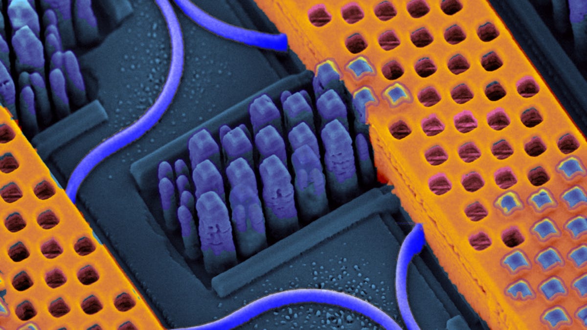
IBM has advanced the technology of silicon photonics, fabricating a microchip that has built-in components to send and receive data over optical links.
Researchers have built optical data links into chips before, but IBM's move is notable because it uses conventional chipmaking equipment geared for chips with 90-nanometer features. Today's chips use metal wires to exchange data, but optical links offer the potential of higher transfer speeds over longer distances.
The chip can include several optical components including wavelength division multiplexers that let the chip send and receive signals with multiple frequencies of light, an approach that lets more data be sent over the same channel in a given amount of time.
The IBM chip can handle data rates of 25 gigabits per second, and the researchers expect to increase that through technology improvements and by building multiple communication channels that work in parallel.
The research is part of IBM's continuing effort to improve computing performance despite Moore's Law challenges.
IBM expects the technology to benefit large-scale systems -- supercomputers, multiple servers linked together, or the data-pathway "backplanes" within servers. It's not unusual for higher-end server technology to trickle down to consumer products, though.
The 90nm process IBM used isn't as advanced as the 22nm one that Intel uses for its latest "Ivy Bridge" generation of processors found in higher-end PCs today. But IBM's approach is the first time silicon photonics has been built into chips with a process size less than 100nm, the paper said. (A nanometer is a billionth of a meter; about 1,100 elements of 90nm chip circuitry could fit side by side across the diameter of a human hair.)
IBM's approach also makes efficient use of electrical power, an important consideration given the power limits processor and computer designers face today.
Big Blue reported the results in a 24-author paper for the IEEE's International Electron Devices Meeting.