IBM brings carbon nanotube-based computers a step closer
Helping the hunt for something to replace silicon transistors, Big Blue researchers have found a way to precisely place carbon nanotubes -- or rather, to encourage them to place themselves.


- Shankland covered the tech industry for more than 25 years and was a science writer for five years before that. He has deep expertise in microprocessors, digital photography, computer hardware and software, internet standards, web technology, and more.
In the effort to find a replacement for today's silicon chips, IBM researchers have pushed carbon nanotube technology a significant step ahead.
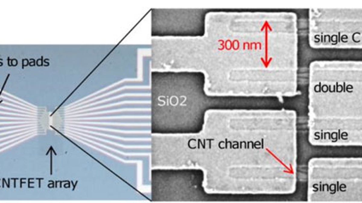
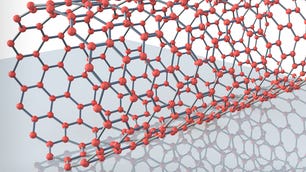
Carbon nanotubes are very small structures made of a lattice of carbon atoms rolled into a cylindrical shape, and a team of eight researchers have figured out a way to precisely place them on a computer chip, IBM announced today. That development allows them to arrange the nanotubes 100 times more densely than earlier methods, a key step in economical chipmaking, and IBM has built a chip with more than 10,000 carbon nanotube-based elements.
The new technique helps improve the nanotubes' chances in the hunt for alternatives once today's silicon transistor technology runs out of steam. Today's chips are made of tiny electrical switches called transistors, and carbon nanotubes are a potential substitute for the silicon channels that carry electrical current in those transistors.
Moore's Law has successfully improved microchips for decades by shrinking chip elements to ever-smaller sizes, and it's got years of life yet in it. Today's Intel "Ivy Bridge" Core processors found in new PCs have transistor elements measuring 22 nanometers, or billionths of a meter, and Intel thinks it can shrink that over several generations of improvement down to 5 nanometers. Beyond that, though, processors will probably need to be built with very different technology.

Carbon nanotubes (CNTs) can have silicon's semiconductor nature, giving them the on-again off-again electrical abilities crucial to making chip transistors. And they have a superb ability to transmit electrons when switched on. But they'll be impractical for computer chips unless chipmakers can find a way to place them very precisely and in large quantities.
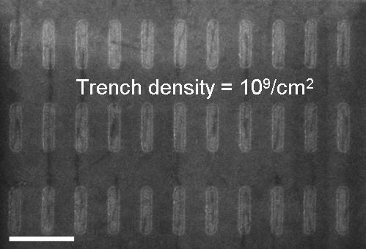
IBM's research, published today in the journal Nature Nanotechnology, uses a combination of chemical tricks that collectively mean chipmakers can place individual nanotubes where they want in special trenches. And they reached a density of a billion nanotubes per square centimeter when constructing their carbon nanotube field-effect transistor (CNTFET) devices.
"This new ability to accurately place individual, aligned CNTs at a high density enables the fabrication of a large number of single-CNT transistors," the researchers said in the paper. "Using the placement method, we fabricated arrays of CNTFETs (designed with one trench per channel of a device) and electrically characterized more than 10,000 CNT devices on a single chip."
Carbon nanotubes show promise, but they're only one candidate for the supposed post-silicon era of computing. Other options include thin ribbons of carbon lattices called graphene that are closely related to carbon nanotubes; moving from silicon to other elements including indium, arsenic, and gallium; silicon photonics, which uses light instead of electrons to transmit information; spintronics, which uses an electron property spin instead of its charge; and even more exotic possibilities such as DNA computers and quantum computing.
The IBM Research paper is written by Hongsik Park, Ali Afzali, Shu-Jen Han, George S. Tulevski, Aaron D. Franklin, Jerry Tersoff, James B. Hannon, and Wilfried Haensch, and their approach requires multiple techniques.
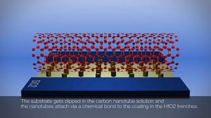
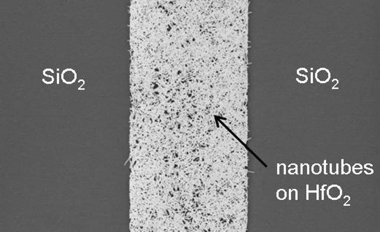
The first step is preparing the wafer -- the same basic substrate used to build conventional microprocessors today. One layer on top consists of hafnium oxide, and then on top of that is a particular pattern of silicon dioxide. IBM's approach leaves thin channels in the silicon dioxide where the hafnium oxide is exposed.
The hafnium oxide is then coated with an extremely thin layer of a chemical called -- brace yourself -- 4-(N- hydroxycarboxamido)-1-methylpyridinium iodide. That's NMPI for short.
The next step is preparing the nanotubes. They're wrapped in a soaplike chemical called a surfactant called sodium dodecyl sulfate that lets them be dissolved into water, then the wafer is immersed in the solution.
The surfactant and the NMPI attract each other chemically, binding the carbon nanotubes to the hafnium oxide trenches. IBM's method can be used to place the nanotubes, correctly aligned, into a grid of narrow trenches. The trenches are 200nm apart in one dimension and 500nm apart in the other dimension, which is how IBM gets the density of a billion nanotubes per square centimeter.
IBM also built a separate device that actually wired the carbon nanotubes so their properties could be measured electrically.
IBM isn't promising the technique will be commercially viable, but some optimism shows through in the paper -- in particular because the process is compatible with current chipmaking technology.
"This new placement technique is readily implemented, involving common chemicals and processes, and provides a platform for future CNTFET experimental studies," the paper said. "Furthermore, these results show that CNT placement via chemical self-assembly is a promising approach for developing a viable CNT logic technology compatible with existing semiconductor fabrication."