AMD pays for IBM know-how in battle with Intel
AMD is leaning increasingly on IBM as it battles with Intel for chip manufacturing process supremacy.


AMD is leaning increasingly on IBM as it battles with Intel for next-generation microprocessor manufacturing leadership. And the payout to IBM is significant.
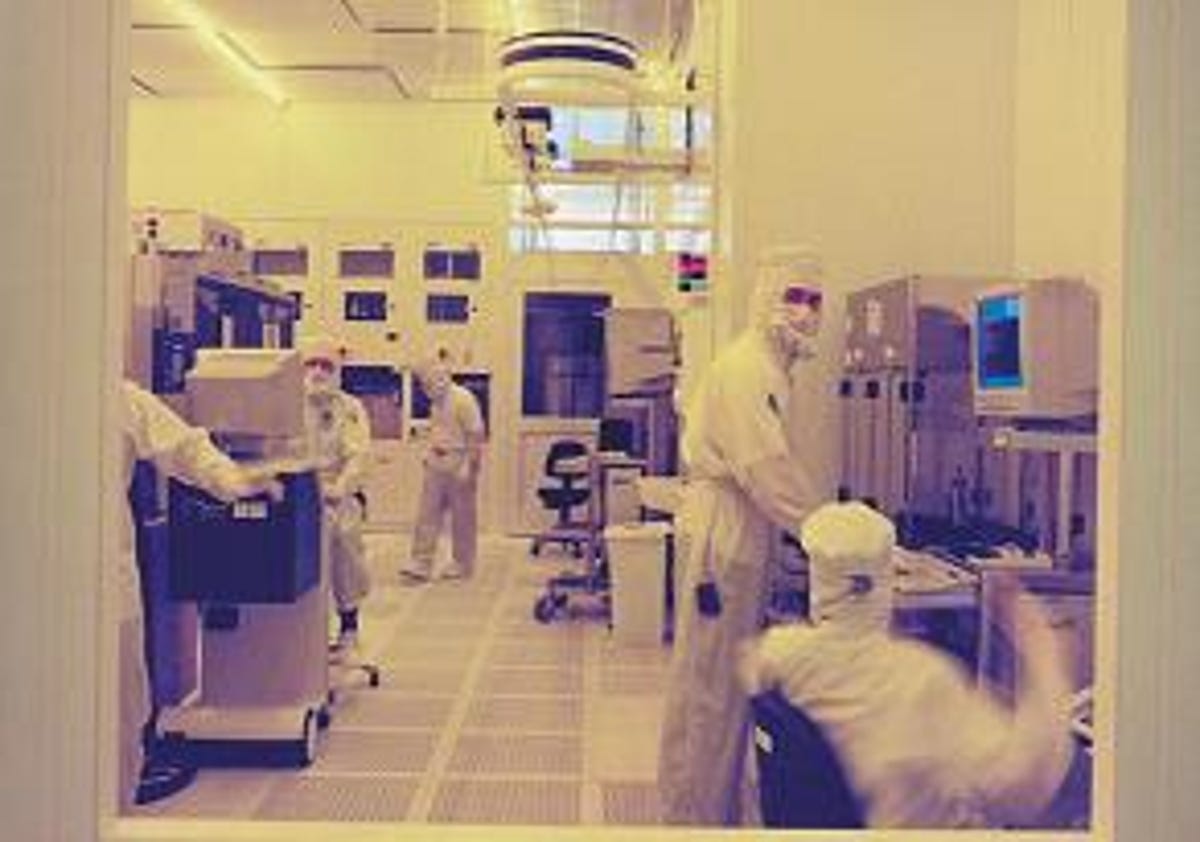
First some background: On Tuesday, AMD announced that IBM had successfully produced a working test chip using next-generation Extreme Ultra-Violet (EUV) lithography for the critical first layer of metal connections across an entire chip. Previous projects utilizing EUV produced working chip components on only a very small portion of the chip.
Why EUV? The size of transistors and the metal lines that connect them is directly related to the wavelength of light that is used to project a chip design onto a wafer. EUV lithography uses a wavelength of 13.5 nanometers (nm), significantly shorter than today's 193nm lithography techniques, allowing the march toward smaller and smaller chip features to continue (though EUV has its own set of problems discussed below). EUV is currently targeted at the 22nm generation of chips, due in three to five years. Intel, a few years back, was targeting EUV for the 45nm generation of chips but abandoned it.
According to the Tuesday announcement, IBM and its partners patterned the first layer of metal interconnects (between the transistors), then, after other processes, the EUV device structures underwent electrical testing at AMD, with transistors showing characteristics consistent with those of test chips built using more standard techniques, the two companies said.
This development follows a series of joint disclosures over the past six years that highlight the crucial expertise that IBM provides to AMD. The two companies began cooperating on advanced chip manufacturing in 2002, when AMD was having trouble with silicon-on-insulator technology, or SOI. AMD got SOI to work with help from IBM and they have been renewing agreements periodically since then. First, in September 2004, to include development of technologies through 2008 for 32nm manufacturing and then again, in November 2005, the agreement was extended through 2011 for the 22nm process. In other areas, AMD is now cooperating with IBM on "high-k/metal gate" transistor technology for next-generation 32nm chips--a technology that Intel is employing in its current 45nm chips.
This kind of know-how is not cheap. AMD's 2007 10K form says the following about the agreement that extends to December 31, 2011: "We anticipate that, under this agreement, we will pay fees to IBM of approximately $400 million in connection with joint development projects between 2008 and 2011."
Even with the substantial payout of $400 million, AMD goes on to say in the 10K that a termination of the agreement "could significantly increase our research and development costs, and we could experience delays or other setbacks in the development of new process technologies, any of which would materially adversely affect us."
Here's the challenge for AMD. Intel's R&D budget dwarfs AMD's. Intel spends about $6 billion per year on R&D, AMD about one-sixth of this. On the manufacturing front, it's even more of a mismatch. For the 45nm generation of chips alone, Intel plans to eventually have four plants making 45nm processors, which Intel is currently manufacturing commercially. AMD doesn't even have 45nm out the door yet (commercially) and needs a chip manufacturing heavyweight like IBM to stay in the running.
As with any collaboration, part of the impetus is to reduce costs. AMD's work with contract manufacturer Chartered Semiconductor is another cost-saving measure. And AMD is by no means the first company to go outside for help and farm out development and manufacturing, said Don Scansen, a semiconductor technology analyst at Semiconductor Insights. But AMD may do more of this as it continues "to get hammered by analysts and the stock market," said Scansen. "IBM is shouldering most of the process development work out of the Common Platform partners--including AMD."
"IBM is a critical part of AMD's Asset Smart manufacturing (and) R&D strategy," an AMD spokesperson said. "By sharing the R&D cost for semiconductor process technology across the membership of the IBM Alliance, each of the parties, including AMD, get access to leading-edge manufacturing technology."
On its Web site, AMD lists transistors, chip connection, packing, and lithography as areas of collaboration. Much of the collaboration takes place at the Albany Nanotech Center. Not coincidentally, Albany is the same spot where AMD has plans to build a chip plant. The chipmaker said recently that if it decides to go forward with the $3.2 billion fabrication plant, construction would start next January, according to a recent report at Timesunion.com.
IBM has a state-of-the-art manufacturing line in East Fishkill, N.Y.--about 90 miles away from Albany--among other locations.
All this collaboration between IBM and AMD means of course that future manufacturing hurdles are high--for everybody. Including Intel, which has delayed procurement of an R&D EUV lithography tool from Nikon, according to a report in EE Times, casting doubt on the viability of EUV at Intel.
From this perspective, the IBM-AMD EUV statement could be seen as promising for AMD. "AMD's ability to get a full chip done with an EUV tool is pretty significant," Scansen said. Some have even been speculating that EUV would not be ready for 22nm, he said. "(But) this announcement might suggest that development is quickening."
AMD and IBM said Tuesday that the next step in proving viability of the EUV lithography for production will be to apply it not only to metal interconnects but to all critical layers to show that an entire working microprocessor can be made utilizing EUV lithography.
Intel has other ideas on how to get to 32nm and beyond using more conventional lithography and "clever design tricks," according to Scansen. And Intel is already moving forward aggressively with 32nm. The company will switch to immersion lithography at 32nm on a "couple of critical layers," according to a statement made in December of last year by Brian Krzanich, vice president and general manager of manufacturing and operations at Intel. The more traditional dry lithography will still be used on less critical layers.